![Architectures and basic properties of photodetectors based on lead sulfide colloidal quantum dot (PbS CQD) photodiode arrays[35, 76, 77, 94, 83-90].](/storage/images/resized/KMx2xLnOOe45w4VWlJrkVpkx8FfHnOHNeaZjsS15_xl.webp)
![Key characteristics of few-element photoresistive structures based on PbS, PbSe, HgTe and HgSe CQDs[177, 156-163, 179-182].](/storage/images/resized/EtnYIubuAFCCdBFtuMkBDuzg2zvOtIjmZVt9xWdc_xl.webp)
![Properties of photovoltaic sensors based on HgTe, PbS and PbSe CQDs[36, 70, 76, 191, 192, 195, 197, 199, 200, 202, 205, 214, 215].](/storage/images/resized/sNWHv3MnFmaLdbBYsrQVP8hUDIILR3lxOi8D9s5K_xl.webp)
![Selected characteristics of field-effect phototransistors based on HgTe, PbSe and PbS CQDs[227, 231, 232, 220-223, 235-237, 239-241].](/storage/images/resized/fDRqPgwCo8jIhoxZ8ecAmodLOBBlV2J7mC11dzsC_xl.webp)
![Properties of optoelectronic night vision devices (NVD) based on PbS colloidal quantum dots[36, 76, 359, 360].](/storage/images/resized/833kN3Zfz3T21GQrGoOA5wfpQDsTo7RUzfz4AyeM_xl.webp)
![Hybridization of a p-n-n+ avalanche photodiode with the input to silicon readout circuit by the HDVIP process without using columnar (or spherical) indium bumps (in relation to the CdTe/ HgCdTe array). The Figure was created by the authors using published data[52-54].](/storage/images/resized/5h99CwXi73pYLXslYWX8eOOXN1oHIuy0DHy1ANZc_xl.webp)
![Photosensitivity spectra of some photocathodes used in modern EOCs[56].](/storage/images/resized/aTOxYy5aSTBcgxJ505vAZv3FggTFbcQzMkKDRByq_xl.webp)
![Temperature dependences of the conductivit G of colloidal quantum dot arrays: (а) CdSe CQDs in the G–1/T1/4 coordinates[131, 133]; and PbS CQDs in the (b) G–1000/T and (c) G–1/T1/4 coordinates[134].](/storage/images/resized/godNgB85iqqR5uW2I2BjiL6fzIBssysV00jgEhYQ_xl.webp)
![Spectral dependences of absorption in colloidal quantum dots of Group II, IV and VI elements: (a) PbS[146]; (b) PbSe[147, 151]; (c) HgTe[148]; (d) HgSe[149]; (e) HgS[150]; the CQD diameter in nanometres is indicated near the curves.](/storage/images/resized/x49BRdsZ7U76VmMXbxn0wSPFZ8JisJDj7UTWgd13_xl.webp)
![Architecture of field-effect phototransistors: (a) based on HgTe CQDs with the structure Si/SiO2/HgTe CQD (/Au)[220] and (b) Si/SiO2/MoS2 (/Au)/TiO2/HgTe CQD[221].](/storage/images/resized/ZJADSAqYfeOMblSRNIWDc58N2eKEyBA3KIvfihuu_xl.webp)
![Field-effect transistor (Si)/SiO2/HgTe CQDs/PMMA[222].](/storage/images/resized/t5Zd1oBoH5UDQfUj8WiVHtb61VbxcmZPaYzTRp8F_xl.webp)
![Formation of n-butylamine complex with mercury chloride[289].](/storage/images/resized/dQZ4mipaHeJIdFcDeUBzFHxaBN3iZWVwgeFdaBkQ_xl.webp)
![Effect of the growth time on the morphology of PbS CQDs[329].](/storage/images/resized/3Po9MrEgOtRHg0BYQEEdC7SgKAWoti89MwCSp6pK_xl.webp)
Keywords
Abstract
Photosensing based on colloidal quantum dots (CQDs) is a rapidly developing area of infrared photoelectronics. The use of colloidal quantum dots markedly simplifies the manufacture, decreases the restrictions to the pixel pitch of the photosensitive elements, and reduces the production cost, which facilitates the wide use of IR sensors in various technological systems. This paper is the first exhaustive overeview of the architectures, methods of manufacturing and basic properties of photonic sensors based on colloidal quantum dots of compounds of Group II, IV and VI elements. Characteristic features of the synthesis and roles of the ligands and CQD morphology in the design of photosensors are considered in detail. The structures of photoresistive, photodiode and phototransistor elements based on HgTe, HgSe, PbS and PbSe CQDs, which are sensitive in various spectral ranges, are described. The main parameters of the most advanced optoelectronic devices based on colloidal quantum dot structures are presented. The key trends in the development of this area are analyzed.
The bibliography includes 361 references.
1. Introduction
The environment is perceived by humans mainly by vision and hearing organs, with 70% of information being gained by vision. Despite the unique characteristics of the human eye as an optical photosensor[1], it can perceive only things in a rather narrow range of electromagnetic radiation wavelengths, from ~0.38 μm to ~0.72 μm (visible region), while leaving subjects in X-ray (10–6 – 10–2 μm), ultraviolet (0.1 – 0.4 μm) and infrared (0.8 – 100 μm) electromagnetic wavelengths beyond the visibility.
The attempts to fabricate devices that would detect and visualize ultraviolet and infrared radiation sources, which were actively started after the World War II, initiated a new research area called optoelectronics; the milestones of its development have been described in a number of publications[2-6]. Optoelectronic devices form the basis for night vision, thermal imaging, infrared direction finding, laser location, optical data transmission and other systems. Of particular interest are research and development related to the elemental base of modern optoelectronics, that is, photosensors sensitive to near-infrared (NIR, 0.8 – 1.0 μm), short-wave infrared (SWIR, 1.0 – 3.0 μm), mid-wave infrared (MWIR, 3 – 5 μm), long-wave infrared (LWIR, 8 – 14 μm), very long-wave infrared (VLWIR, 14 – 30 μm), and extremely-long wave infrared (30 – 100 μm) electromagnetic radiation.
There exist a variety of approaches to the design of photosensing devices. The design and manufacturing of photosensors for the wavelength range of 0.4 – 0.9 μm covering the visible and near-infrared light are largely related to image intensifiers, which use the external emission of electrons excited by absorption of photons focused by an IR lens on the photocathode of an electro-optical converter[6].
For spectral wavelengths λ > 0.9 μm, development of photosensors is mainly associated with the solid-state semiconductor photoelectronics based on the internal photoelectric effect. In photonic sensors, the observed signal is the measure of excitation by incident photons of the electronic system of a semiconducting material forming the photosensitive structure. There are a number of architectures for photonic elements that form the basis of virtually all types of photosensors used in both the infrared and ultraviolet and visible regions. Most often, single-area and line photosensors with no more than 200 elements are designed on the basis of photoresistors. There are also examples of photodetector arrays. For example, a latest-generation photodetector array is a two-dimensional GaAs/AlGaAs-based quantum well infrared photodetector (QWIP), which uses the photoresistive effect[4]. Energy barrier photodiodes can be based on both homo-(p-n) and heterojunctions of various types (P-n, N-p, P-p, n-N), Schottky barriers, p-i-n homo- and heterojunctions, avalanche gain, bariode heterosystems, injection diodes, etc. Most of modern 2D photodetector arrays are based on photodiodes. Depending on the required sensitivity range, operating temperature and operation speed, photodetectors are manufactured using various materials such as Ge and Si (in particular, those doped with Hg, Au, Zn, B, As, P, Al, In, S, Mg, and other ions), PbS, PbSe, PbTe, CdS, CdSe, InSb, InP, GaAs, InAs, InGaAs, CdHgTe, and so on[7-9]. In the far-IR region, apart from photodetectors, non-selective thermal detectors (microbolometers) are often used[4].
The modern trend of development of solid-state IR photosensors is associated with the design of 2D photodetector arrays. Currently, they are being developed virtually for all semiconductor compounds that have a sufficient photosensitivity in the ultraviolet and near-, mid- and far-IR regions and in the terahertz (THz) region. These camera arrays (N × N format in systems without image scanning) and TDI subarrays [M × N format, where М = 2, 4, 8, 12, for the time delay and integration (TDI) mode in optical mechanical scanning systems) are referred to as second-generation solid state photosensing devices[4].
A considerable progress has been made in the development of second-generation solid-state semiconductor photosensors. Imaging arrays comprising more than a few million elements with 1280 × 1024, 1920 × 1080, 2048 × 2048, and 4096 × 4096 formats (Figure 1) have now been fabricated for the main infrared spectral regions, 0.9 – 1.7 μm, 3 – 5 μm and 8 – 12 μm, corresponding to the transparency windows of the Earth’s atmosphere[10, 11]. Lately, special attention has been paid to the development of multiband devices sensitive in several spectral regions. The possibilities of increasing the operating temperature are being investigated. The ways for reducing size, weight and power consumption of photosensors [size-weight-and-power (SWaP) concept of development] are being explored.
![[{"id":"YBs-X8Yt5Z","type":"paragraph","data":{"text":"Photosensitive element based on Cd<sub>x</sub>Hg<sub>1–x</sub>Te photodiode (l<sub>c</sub> = 2.5 µm) of 4096×4096 format for the James Webb space telescope; l<sub>c</sub> is the cut-off wavelength[[ type=\"anchor\" referenceId=\"3592\" ]]."}}]](/storage/images/resized/hORd3rY7WxIzSdYKTnBTIfEn7U63TYpzxSHIX3Gg_xl.webp)
Meanwhile, in recent years, certain drawbacks of the currently developed technologies of infrared and ultraviolet photosensors based on solid-state semiconductor electronic materials, structures and approaches have become more obvious, and they restrict some applications of the developed devices. First of all, this refers to complexity of integrating photosensor arrays with microelectronic readout integrated circuits (ROIC), which restricts the format and the minimum size of photosensitive elements; high cost of the starting semiconductor materials; the need to use cryogenic operating temperatures; and sophisticated and expensive manufacturing equipment, resulting in high cost of the final product. This stimulates the search for alternative approaches to the production of components for optoelectronics, new photosensitive materials and techniques for multi-element photosensors and photosensor arrays operating in ultraviolet and infrared spectral ranges.
The last decades witness the rapid increase in the number of studies directed towards the design of photosensors using low-dimensional materials and structures. Examples are structures based on graphene and graphene-like and related 2D nanomaterials, non-graphene 2D materials composed of Group IV, V, VI and IIIa elements, nano-sized layers of topological insulators like bismuth telluride, etc[12-15]. The design of photosensors based on type-II superlattices (T2SL) is being successfully developed. The T2SL structures are alternating nano-sized layers with different band-gap semiconductors (InAsSb/InSb, InGaAs/GaAsSb, InAs/GaSb, PbTe/PbS, PbTe/ SnTe)[16]. The properties of T2SL structures often eliminate some drawbacks inherent in solid-state semiconductor photosensors based on 3D single crystals and epitaxial layers, e.g., increase the sensor operating temperature owing to significantly lower dark currents.
The last two decades witnessed the appearance a new trend in the design of photosensors, particularly, the use of so-called colloidal quantum dots (CQDs), the spectral properties of which are specified by the average size of semiconductor nanoparticles, which is varied in the 2 – 50 nm range. Meanwhile, the width of the luminescence spectrum of a single nanoparticle at room temperature is only 20 – 30 nm. Thus, quite a small set of luminescent quantum dots based on AIIBVI, AIIIBV or AIVBVI type semiconductors easily cover the spectral range from 350 to 3500 nm owing to variation of their size[17, 18].
The size dependence of the absorption and luminescence spectrum properties of ultradisperse semiconductors was first demonstrated in 1981 by A.I.Ekimov and A.A.Onushchenko from the S. I.Vavilov State Optical Institute, in relation to CuCl nanoparticles grown in multicomponent silicate glasses during thermally initiated diffusion phase decomposition of a supersaturated solid solution, and theoretically substantiated by Al.L.Efros and A.L.Efros[19, 20]. Independently, L.E.Brus the same dependence for a CdS dispersion[21, 22]. Over the following several years, this effect was experimentally detected and confirmed for ultradisperse particles of a number of semiconductors such as CdS, CuBr, CdSe, PbS, ZnS, Zn3P2, and Cd3P2[23-28]. The term ‘quantum dot’ (QD) was first introduced in 1988 by Reed et al.[29], who studied the electron transport in quasi-zero-dimensional semiconductor nanocrystals and showed that an electron behaves in a nanocrystal as in a three-dimensional potential well. When the nanocrystal size becomes smaller than the exciton Bohr radius, the continuous spectrum of allowed charge carrier energies (characteristic of the conduction and valence bands of bulk crystals) is replaced by a discrete spectrum. The size of such nanocrystals consisting of 103 – 105 atoms and called quantum dots was found to range from 2 to 50 nm. A similar size quantization of the energy spectrum was also observed for nanocrystals formed as nanoparticle dispersions in organic or aqueous solutions. These nanocrystals are called colloidal quantum dots.
In 1993, Murray, Norris and Bawendi[30] proposed a facile and highly efficient chemical method for the synthesis of quantum dots, which was called high-temperature colloidal synthesis. This method not only opened up new opportunities for studying CQDs, but also clarified the real prospects for their practical applications.
As a recognition of the significance of this research area and priority of the pioneering studies that initiated a new field of photonics that actively develops now, Louis Bruce, Alexey Ekimov and Alexander Efros were awarded the R.W.Wood Prize in 2006, while in 2008, Louis Bruce was awarded the Fred Kavli Prize in nanoscience. In 2023, Moungi Bawendi, Louis Bruce and Alexey Ekimov won the Nobel Prize in Chemistry.
The CQD-based approach to the fabrication of infrared photodetector arrays, which has actively developed in recent years, markedly simplifies the technology, reduces the pixel pitch limitation for the photosensitive elements and considerably reduces the cost of photodetector arrays[31, 32]. The vigorous development of this area in the last few years resulted in the fabrication of the first commercial imagers and cameras based on them, which operate in the spectral range from 0.4 to 2.1 μm[33-36].
A number of reviews published over the past few years generally address the use of CQDs for a wide range of applications[37, 38]. In 2023, Mamiyev and Balayeva[39] considered various applications of PbS-based CQDs. The key achievements in the synthesis of PbS CQDs and the fabrication of thin films based on them are addressed by W.M.M.Lin et al[40].
In addition, there are a number of specialized reviews devoted to particular issues of photosensor applications of CQDs. For example, V.Pejovic et al.[41] analyzed the advances in the CQD image sensor technology as of June, 2022. The protosensor applications of PbSe and PbS CQDs are addressed by M.C.Gupta et al.[42] and H.Wu and Z.Ning[43].
Ponomarenko et al.[44] analyzed the architectures of photosensitive elements and described the advances in the CQD-based photoelectronics as of the beginning of 2021.
The present review gives the first comprehensive and detailed account of the architectures, fabrication methods and properties of photonic sensors based on colloidal quantum dots of Group II, IV and VI elements. The review describes the synthetic approaches, the influence of ligands and morphology of various CQDs used in photosensors. Functional diagrams are considered for photoresistor, photodiode and phototransistor elements with absorption layers based on HgTe, HgSe, PbS and PbSe colloidal quantum dots for operation in various spectral ranges, including hybrid elements using functional layers made of 2D materials. The parameters of the best optical devices based on colloidal quantum dot structures as of the beginning of 2024 are given. On the basis of publications of the last few years, we analyze the potential and development trends for the photonic sensors composed of colloidal quantum dots of compounds of Group II, IV and VI elements as one of the most promising new areas of quantum photosensorics.
2. Photosensing devices based on 3D semiconductor structures
2.1. Photosensor arrays based on 3D semiconductor structures. State of the art, benefits and drawbacks
The fabrication of second-generation two-dimensional photodetectors required the development of way for electrical connection (hybridization) of hundreds of thousands and millions of photosensitive elements made of semiconductor materials (Figure 2) with an equal number of microelectronic input devices arranged in a silicon readout integrated circuit (ROIC). This is exemplified in Figure 2, which shows the connection of an indium antimonide photodiode array to silicon ROIC. The development of the hybrid technology started in the second half of the 1970s. This required elaboration of a method for growing indium bumps with size and height variations of approximately fractions of a micrometre; development of special high-precision equipment for the thermocompression bonding of a group of bumps located on a silicon ROIC to a similar group located on an array of photosensitive elements[45]. The above hybridization operation is a key issue for all second-generation photodetector arrays. Using this operation, photonic detector arrays were fabricated, including those of a mega-pixel format, based on InSb (1280 × 1024, 1920 × 1536), InGaAs (1280 × 1024) and CdHgTe (2048 × 2048, 4096 × 4096) photodiodes and multielement AlGaN arrays (320 × 256, 640 × 512)[11, 12, 46-51]. The hybridization technique substantially influences the photosensor quality, since connection defects (bonding disruption between single bumps of the photodiode array and ROIC wafer due to their different heights, high resistance in the contact layer, etc.) give rise to non-functional photosensitive elements.
![[{"id":"--M5fpkVLo","type":"paragraph","data":{"text":"Hybridization of InSb photodiode array with Si ROIC wafer for signal readout and preliminary processing using indium bumps: (a) hybridized photosensitive elements and Si ROIC wafer; (b) two array elements connected by columnar indium bumps to the ROIC input devices (Т1 transistor sources)."}}]](/storage/images/resized/kzlgPQKpWfAea85Y7PemTmGHWUDeukx0MZAYbZ4Y_xl.webp)
The hybridization operations performed using the above-described indium bumps restrict most appreciably characteristics of photosensor arrays for near and short-wave spectral regions of 0.7 – 3.0 μm. The diameter of columnar indium bumps with minor variations of the diameter and height can hardly be made smaller than 3 – 5 μm. Meanwhile, the maximum pixel pitch for photosensitive elements for arrays operating in the 0.4 – 1.7 μm that provides the best spatial resolution for an electro-optical system is approximately 2 μm. For the mid-wave infrared range (MWIR) of 3 – 5 μm, the pixel pitch should be approximately 4 μm. In the design of CdHgTe-based avalanche photodiodes (APD) in the early 2000s, a hybridization method of APD array with Si ROIC without using columnar or spherical indium bumps was developed; this gave so-called high density vertically integrated photodiodes (HDVIPs)[52]. The architecture of an avalanche p-n-n+ photosensitive element based on the CdTe/ HgCdTe pair hybridized by the HDVIP process with silicon readout input is shown in Figure 3[52-54]. The diameter of the vertical via formed by ion etching in CdTe/HgCdTe is approximately 6 μm. However, this hybridization method did not provide the required pixel pitch for photosensitive elements either.
Thus, hybridization of photodiode arrays and signal readout electronic circuits using columnar bumps or via holes (HDVIP method) is not only labour-consuming, requires the use of highly precise and expensive equipment, decreases the percentage yield of acceptable arrays and increases the cost of products, but also limits the pixel pitch of photosensitive elements for arrays not smaller than 3 – 5 μm, which has an adverse effect on the spatial resolution of optoelectronic devices and complexes using such arrays.
2.2. Photosensor devives for near- and short-wave infrared regions: problems and solutions
Unlike the thermal imaging devices operating in the mid (3 – 5 μm) and far (8 – 12 μm) spectral regions and recording the intrinsic radiation of items heated to 240 – 970 K, the devices operating in the 0.7 – 1.0 μm and 1.0 – 3.0 μm ranges record the intrinsic radiation of items heated to temperatures above 970 K and reflected radiation of, first of all, natural sources (Sun, Moon, stars, natural radiation of the night sky). The images obtained using special instruments in these spectral ranges by measuring the radiation reflected from an observed object have shadows and half-tones and thus allow highly accurate recognition of these objects or parts of objects that have no temperature contrast. This is illustrated by Figure 4, demonstrating that only visible (0.38 – 0.72 μm) and short-wave IR (1.0 – 3.0 μm) images make it possible to confidently recognize the facial features and, hence, identify a person[55]. Due to the inevitable differences in the reflectivity of different fabrics and dyes, the range of 1.0 – 3.0 μm makes it possible to distinguish between camouflage outfits of different countries and thus to make the friend-or-foe identification. This indicates the relevance of development of advanced photosensors providing high-quality images in the NIR and SWIR ranges of electromagnetic radiation. The major part of the visible and near-IR ranges is covered by night vision devices (NVD); the photosensors of these devices are represented by generation III and III+ vacuum electrical to optical converters with GaAs-based photocathodes with a negative electron affinity and cut-off wavelength of not more than 0.93 μm and quantum efficiency of approximately 30% (Figure 5, curve 6)[56]. The Sb – Rb – Cs or Sb-K – Cs bialkali photocathodes (e.g., K2CsSb and Rb2CsSb), photocathodes based on GaAsP ternary solid solution, and Na-K – Sb – Cs multi-alkali photocathodes [e.g., (Cs)Na3KSb] (Figure 5, curves 3, 4, 5) have a higher quantum efficiency (30 – 55%), but their spectral sensitivity is limited to the visible and near-infrared spectral regions. The same is true for the super bialkali (SBA) and ultra bialkali (UBA) type photocathodes based on bialkali compounds manufactured by a specific technique resulting in an increase in the absolute sensitivity, but not in an extension of the spectral range[57]. The efforts of the last decades on the search for photocathodes with a cut-off wavelength extended to the short-wave IR (SWIR) region resulted in the development of new-generation photocathodes based on InGaAs and InGaAsP solid solutions and рhotocathodes based on InP/InGaAsP and InGaP/InGaAs heterojunctions with cut-off wavelengths at about 1.6 μm. The greatest progress was attained for photocathodes with InP/InGaAs heterojunction (Figure 5, curve 9). However, the wide use of such devices in night vision technology is hindered by their low quantum efficiency, not exceeding a few percent, and high cost.
![[{"id":"Wne1omtlba","type":"paragraph","data":{"text":"Facial images of the same person in different spectral ranges: 0.4–0.7 µm (visible), 1.0–3.0 µm (SWIR), 3.0–5.0 µm (MWIR) and 8.0–14.0 µm (LWIR)[[ type=\"anchor\" referenceId=\"3879\" ]]."}}]](/storage/images/resized/jw6cceNqHYlnMmuzyrhz65mzVyVrFKyfWLwj0CZn_xl.webp)
The key NVD parameters (range of vision, probability of detection and recognition, noise protection and noise resistance, power consumption, etc.) depend on the external conditions under which NVD is used. The key external conditions of NVD operation (in passive systems without artificial light source) include
— spectral composition and level of the natural night illumination (NNI);
— atmospheric parameters along the observation track;
— atmospheric haze;
— brightness coefficients of natural entities and observation targets.
The natural night illumination of the Earth’s surface at different times of the day, in various regions, at different weather conditions, etc. has been investigated for many years. Generally, the results of these studies can be summarized as follows[58-60].
The major source of NNI is moonlight, which provides spectral irradiance of 1.8 × 10⁻³ W m–2 μm–1 at λ ≈ 0.7 μm near the Earth’s surface; for the wavelength λ ≈ 1.6 μm, this value decreases to approximately 1.2 × 10⁻³ W m–2 μm–1 (Figure 6a)[58]. The spectral irradiance generated by stars in the visible region in the wavelength range of 1.4 – 1.8 μm is much lower. On a clear moonless night, the main natural sources of illumination are the airglow, starlight and zodiacal light. The main contribution to the ground illumination is made by airglow (Figure 6b)[58]. The night airglow is caused by various processes taking place in the upper atmospheric layers: recombination of ions formed upon рhotoionization during daytime under the influence of the solar radiation; reactions between oxygen, nitrogen and hydroxyl OH– accompanied by photon emission; luminescence caused by the passage of cosmic rays in the upper atmosphere; reactions involving lithium and sodium; and combination reactions between nitrogen and oxygen atoms accompanied by photon emission.
![[{"id":"RSeXR9O1bU","type":"paragraph","data":{"text":"Spectral irradiance of natural night illumination: (a) with a full Moon; (b) airglow in a moonless night[[ type=\"anchor\" referenceId=\"3882\" ]]."}}]](/storage/images/resized/NLeFWdcVDKkH2JeaVn92o789xX3Y606HwLG1eMfb_xl.webp)
Comparison of these characteristics for the 0.4 – 0.9 μm and 1.4 – 1.8 μm spectral ranges shows that[61]
(a) the spectral irradiance from NNI regularly increases on going from the visible [from λ ≈ 0.38 μm (violet) to 0.78 μm (red)] to IR spectral region (λ ≥ 0.9 μm); indeed, in the absence of moonlight, the average spectral irradiance for λ = 0.6 – 0.8 μm is (1.5 – 3.0) × 10–5 W m–2 μm–1, while in the 1.4 – 1.8 μm wavelength range, it increases to (6.0 – 7.0) × 10–4 W m–2 μm–1;
(b) air transparency is much higher in the near-IR range than in the visible range; for example, for the meteorological visibility SM = 10 km, transmittance of a 1 km thick atmospheric layer is 0.72 at λ = 0.6 μm and 0.93 at the centre of the transparency window (1.4 – 1.8 μm);
(c) brightness of the atmospheric haze decreases more than 10-fold in the 1.4 – 1.8 μm wavelength range compared with thee visible region;
(d) NNI changes during the night from 10–1 W m–2 to 2.5 × 10⁻⁵ W m–2 (i.e., by almost four orders of magnitude) in the 0.4 – 0.9 μm spectral range, while in the 1.4 – 1.8 μm range, this change is from 1.6 × 10⁻¹ W m–2 to (3 – 4) × 10–3 W m–2; (e) the contrast (observation target/background) is 1.4 – 1.5 times higher in the 1.4 – 1.8 μm wavelength range than in the 0.4 – 0.9 μm range.
A comparative estimation of the ranges of vision \( L_1 \) and \( L_2 \) for two NVDs with identical optical systems, but different spectral sensitivity ranges was reported by Gusarova et al[61]. The \( L_1/L_2 \) ratio was calculated by the formula:
where \( L_1 \) is the distance of action of NVD at which the detection of an object ensures recognition, \( K_1 \) is contrast, \( \tau_{a\lambda} \) is the spectral atmospheric transmittance between the target and the observer, \( S_{1\lambda} \) is the relative spectral sensitivity of a conventional detector operating in the 1.4 – 1.7 μm range, equal to \( S_{1\lambda}/S_{1\lambda max} \), \( E_{\lambda} \) is the spectral irradiance on the target surface; \( L_2 \), \( K_2 \), \( S_{2\lambda} \) are the same parameters for EOC with the sensitivity range of 0.4 – 0.9 μm. The estimated \( L_1/L_2 \) ratios indicate that for a low illumination level on a horizontal track, \(E_H = 1.4 \times 10^{–3} lux \) and meteorological visibility \(S_M = 2.5 km \), the \( L_1/L_2 \) ratio is 13, while for \(S_M = 20 km \), \( L_1/L_2 = 8 \) .
This estimate convincingly demonstrates the considerable advantage of photonic sensor arrays with cut-off wavelength λc of approximately 1.8 – 2.0 μm for night vision devices. Meanwhile, the manufacture of these devices all over the world is currently based on vacuum electrical to optical converters operating in the range of 0.4 – 0.9 μm.
The solid-state photonic sensors with cut-off wavelength λc ≈ 1.8 μm are now largely manufactured using semiconductor solid solutions In053Ga047As as epitaxial layers grown on InP substrates for which there exist a technique for the fabrication of photodiodes with a photosensitive element pitch of 12 – 15 μm and an assembly technique with signal readout and processing integrated circuits made of silicon by means of indium bumps[11, 12, 48, 49]. Due to the active optical absorption of visible light, the InP substrate restricts the short-wavelength cut-off to approximately λ ≈ 0.9 μm. In order to extend the photosensitivity range to the visible part of the spectrum, various methods are used for thinning or eliminating the InP substrate[62-64]. This may provide a photosensor quantum efficiency of approximately 60% at λ = 0.5 μm[64]. In recent years, considerable progress was also attained in the development of methods for reducing the pixel pitch for InGaAs-based photodiode arrays by switching from the indium bumps to copper-based planar microcontacts (cupper-to-copper microcontacts), the basic diagram for which is shown in Figure 7[48, 64-68]. However, this type of hybridization does not eliminate the above-noted drawbacks of photosensor arrays based on 3D materials, related to the necessity to use highly precise and expensive equipment and high labour consumption, resulting in high cost of products.
![[{"id":"3zRit2XgTA","type":"paragraph","data":{"text":"Hybridization of a 1280×1024 photodiode array based on InGaAs solid solution semiconductor with Si ROIC: (a) using indium bumps (17 µm pitch); (b) using planar Cu–Cu microcontacts (5 µm pitch); (c) TEM image of planar Cu–Cu microcontacts (3 µm pitch). The Figure was created by the authors using published data[[ type=\"anchor\" referenceId=\"3872,3888,3890\" ]]."}}]](/storage/images/resized/cYZAK5SYKpCDtMU0Li3TgNtnNXXXhSwcj4BqDatB_xl.webp)
3. Photonic sensor arrays for the near- and short-wave spectral regions based on colloidal quantum dots
Quite a few recent publications are devoted to the design of photosensitive elements operating in the near and short-wave IR regions using CQD-based low-dimensional structures[69-74]. The use of CQD-based structures as the element base of photosensorics provides a number of characteristics that are of fundamental importance for the key technology of photodetector arrays. The most significant of these characteristics are the following:
— CQD-based arrays are completely free from In or Cu metal microcontacts, usually utilized for connecting the photodiode arrays to silicon multiplexers; CQD-based photosensitive layers can be formed by spin-coating, jet or aerosol printing at moderate temperatures directly on the surface of input devices of silicon ROIC (Figure 8)[75];
— currently, there are mega-pixel (2.1 MP) CQD PbS array formats amounting to 1920 × 1080 at a 15 μm pitch[76]; however, the pixel pitch and format are restricted only by those of the silicon multiplexor; therefore, the fabrication of supermegapixel devices is possible in the future;
— the two smallest pixel pitches known for SWIR sensors (1.62 and 1.82 μm) were implemented in ROIC used with CQD-based photodiodes in which there are no limitations related to the minimum size of indium bumps[77, 78]; — a 640 × 512 array based on HgTe CQDs with a pitch of 15 μm for the SWIR spectral range is markedly less expensive than the same array based on the epitaxial InGaAs heterostructure[32];
— wide range of spectral sensitivity Sl(l) of PbS nanocrystal; furthermore, the right edge of Sl(l) dependence can be controlled by varying the quantum dot size via variation of conditions of CQD synthesis[69, 79].
The first attempts of using PbS nanocrystals as quantum dots for recording electromagnetic radiation in the wavelength range of 0.975 – 1.3 μm were undertaken in 2004 and reported by McDonald et al[80].
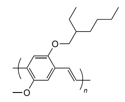
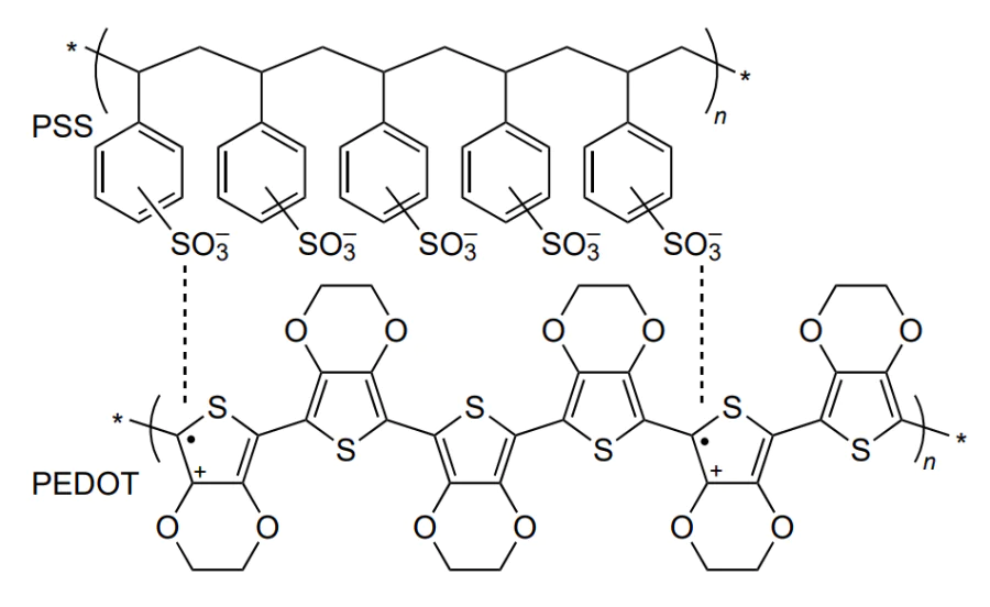
The authors[80] described photoresistors in which PbS nanocrystals distributed throughout the MEH-PPV polymer served as the photosensitive medium. The photoconductivity spectra of the MEH-PPV : PbS CQD nanocomposites for variable PbS CQD size showed maxima at 0.98, 1.2 and 1.355 μm wavelengths. The photosensitive layer was deposited on an electrode coated by indium tin oxide (ITO). McDonald et al.[81] described the first photodiode with the ITO/PPV/PbS CQD : MEH-PPV/Mg architecture. In 2009, McDonald et al.[82] described the architecture of a photosensitive element obtained by deposition of 256 × 256 pixel array on Si ROIC from a solution. The photosensitive element consisted of photodiodes based on bulk heterojunctions produced by mixing PbS colloidal quantum dots with two organic compounds, poly(3-hexylthiophene-2,5-diyl) (P3HT) and phenyl-C61-butyric acid methyl ester (PCBM) (Figure 9)[82]. A better contact between the photosensitive layer and the ITO electrode was attained by using an interlayer based on the poly(3,4-ethylenedioxythiophene) (PEDOT) : poly(styrene sulfonic acid) (PSS) composite. Since then, lead sulfide colloidal quantum dots have been recognized as one of the most promising materials of IR photosensorics.
![[{"id":"19741OjbNd","type":"paragraph","data":{"text":"(a) Architecture of a photosensitive element based on the PbS CQD:P3HT:PCBM bulk heterojunctions; (b) structure of PCBM (phenyl-C61-butyric acid methyl ester)[[ type=\"anchor\" referenceId=\"3906\" ]]."}}]](/storage/images/resized/leGIqoJhFvIFQ8OZJisJqrcnfh8s9OXBhDbGuErZ_xl.webp)
Lately, two architectures have been most popular for the development and fabrication of photodetector arrays based on PbS colloidal quantum dots, particularly, one using the energy barrier of the PbS CQD/C60 heterojunction (Figure 10, Figure 11)[75, 83-89] and one using the energy barrier across the p-PbS CQDs/n-TiO2 contact (Figure 12)[90-93]. The former architecture was used to design 640 × 512, 1280 × 1024 and 1920 × 1080 photodiode arrays with an extended sensitivity range from 0.35 to 2.1 μm and photosensitive element pitch of 15 μm, which are commercially distributed[76, 83-89]. The latter architecture was used to design image sensors with 640 × 480, 640 × 512 and 768 × 512 formats and a reduced pixel pitch of 5 μm[90]. Using this architecture, photodetectors with very small pixel pitches of 2.1 and 1.82 μm were studied[34, 91-93]. A pixel pitch of 1.62 μm was attained for photosensitive elements based on PbS CQDs with microlenses and copper reflective coatings[78].
![[{"id":"Qo-WUl9Uyr","type":"paragraph","data":{"text":"Photosensitive element with an energy barrier at the PbS CQD/fullerene C<sub>60</sub> contact: (a) architecture of a photosensitive element of 1 mm in diameter; (b) energy diagram; (c) current–voltage characteristic of the structure: in the dark (dark) and under illumination (light) from a source with a spectral composition and power of 100 mW×cm<sup>–2</sup> corresponding to solar radiation[[ type=\"anchor\" referenceId=\"3899,3907,3908,3909,3910,3911,3912,3913\" ]]."}}]](/storage/images/resized/LgLmWiBnqlmfehHrbaOgb2Cl4e6LYlF5R7bHAnNc_xl.webp)
![[{"id":"w35-Fsr2nd","type":"paragraph","data":{"text":"Diagram of integration of photosensitive element array based on CQD barrier structure to Si ROIC with the top contact/С<sub>60</sub>/CQD PbS/bottom contact architecture: (a) photodiode array hybridized with Si ROIC; (b) two С<sub>60</sub>/CQD elements electrically connected to the input devices of ROIC (Т1 transistor sources). The energy barrier is formed at the С<sub>60</sub>/PbS CQD contact. The Figure was created by the authors using published data[[ type=\"anchor\" referenceId=\"3899,3912\" ]]."}}]](/storage/images/resized/nB11YxJlKRacQEAiKEA7m7iFPmgUwfeybjM63xv1_xl.webp)
![[{"id":"BSXLIUf77P","type":"paragraph","data":{"text":"Architecture of a 640×512 photosensor array with a 15 µm pitch based on PbS CQDs."}}]](/storage/images/resized/UHwMn3kRsSMOjEYZa6Z7E1FAbyook8kvS587TrBb_xl.webp)
The architecture of a single photosensitive element with a PbS CQD/C60 heterojunction energy barrier is shown in Figure 10a. This is a sequence of nanolayers ITO (top contact)/MoO3 (EBL)/PbS CQD/C60/BCP (HBL)/bottom contact where MoO3 serves as the electron blocking layer (EBL). In the CQD and fullerene C60 layers, photons of electromagnetic radiation are absorbed, excitons appear and decay to give electron – hole pairs, which are separated at the boundary between PbS CQDs and C60. The electrons are transported through the C60 layer, pass through the hole blocking layer (HBL) and are collected by the aluminium bottom contact. 2,9-Dimethyl-4,7-diphenyl-1,10-phenanthroline [bathocuprine (BCP)] acts as HBL. Similarly, holes are transported through the PbS CQD layer, pass through the EBL layer and are collected at the indium tin oxide (ITO) (In2O3)0.9(SnO2)0.1 top contact. The energy diagram of this structure and the current – voltage characteristic (CVC) (in the dark and under illumination from a radiation source with a spectral composition corresponding to solar radiation) are shown in
![[{"id":"KFXgVExtCH","type":"paragraph","data":{"text":"Energy diagram (a) and STEM image of the architecture (b) of the ITO (top electrode)/polyTPD (EBL)/PbS CQDs/TiO<sub>2 </sub>:Nb (HBL)/bottom electrode photosensor[[ type=\"anchor\" referenceId=\"3917\" ]]."}}]](/storage/images/resized/YnHqx6HBb3FVQ6Ydu7eZhkLNpxDMMcr5orJXAA5Y_xl.webp)
The energy diagram of the photosensitive element with an energy barrier at the CQD, p-PbS and n-TiO2 contact is shown in Figure 12. This is a sequence of nanolayers: ITO (top contact)/polyTPD (EBL)/PbS CQD/TiO2 : Nb (HBL)/bottom contact, where polyTPD [poly(4-butyl-N,N-diphenylaniline] serves as the electron-blocking layer, and TiO2 is a hole blocking layer. Silver and TiN layers can be used as the top (transparent) and bottom (non-transparent) contacts[93]. The HBL layer with electronic conductivity is fabricated by doping TiO2 with niobium.
A key characteristic of photosensors is the specific detectivity D* (Table 1)[94]. The B/BCP/C60/PbS CQD/MoO3/ITO photosensors (В is the non transparent bottom contact) are characterized by the detectivity D* of 1.0 × 1012 cm Hz1/2 W–1 (20 °С, λ = 1.4 μm); as the sensor is cooled down to –20 °С, this value increases to 4.0 × 1012 cm Hz1/2 W–1. Figure 13 shows the spectral dependences of the responsivity (A W–1) and the detectivity of a mega-pixel PbS CQD photosensor (1920 × 1080) with the long cut-off wavelength λc = 1.9 μm[33, 76].
![[{"id":"GwD5WI1BI9","type":"paragraph","data":{"text":"Spectral dependences of the responsivity and (a) and specific detectivity (b) of a 1920×1080 photosensor array (15 µm pixel pitch)[[ type=\"anchor\" referenceId=\"3900\" ]]."}}]](/storage/images/resized/tdDyKzsIQaOoViVCi29WRKQuKh15UpPoehT42wG9_xl.webp)
The key characteristics of the above-described photosensors based on PbS colloidal quantum dots are summarized in Table 1[35, 76, 77, 83-90].
In 2022, Gréboval et al.[32] described a HgTe CQD-based photosensor array using photoresistive architecture of photosensitive elements. The 640 × 512 array with a pixel pitch of 15 μm based on HgTe CQDs showed a cut-off wavelength λ = 1.8 μm and quantum efficiency of ~15%[32].
In 2023, Luo et al.[95] described a 1280 × 1024 mega-pixel photodetector based on HgTe CQD photoresistors (15 μm pitch) with a cut-off wavelength of 2.0 μm, responsivity of 0.23 A W–1 and quantum efficiency of ~14% at room temperature[95]. The search for new elements for sensor arrays based on low-dimensional structures and ways to improve them has been intensively carried out in recent years as well[96-103].
A 388 × 288 array with the PbS CQD-based photosensitive layer and readout circuit was studied by S.Goossens et al[104]. The sensor sensitivity and detectivity were 0.3 – 1.0 μm and 1012 cm Hz1/2 W–1, respectively.
4. Electrophysical properties of CQDs and layers based on them
4.1. Electronic structure of CQDs
Colloidal quantum dots are commonly defined as crystalline inorganic particles with a nearly spherical shape and radius R ranging from ~1 to ~25 nm containing hundreds to thousands of atoms. A quantum dot is larger than a molecular cluster, typically containing 10 to 100 atoms and having ~1 nm in size.
Bulk (3D) binary compounds PbS, PbSe and PbTe crystallize in the face-centred cubic lattice of rock salt NaCl (space group \( O_{h}^5-Fm3m \)), which has four atoms in the unit cell[105]. At high pressure, they undergo a polytype transition to a crystal lattice with space group \( D_{2h}^{16}-Pnma \). The energy band structures of lead salts PbS, PbSe and PbTe are very similar. Their Brillouin zones are the same as that of Group AIV elemental semiconductors. In the lead chalcogenides PbS, PbSe and PbTe with cubic symmetry (\( O_h \) point group of symmetry), the first Brillouin zone has a system of eight semi-ellipsoids of equal energy, the symmetry axes of which coincide with the [111] directions. The centres of ellipsoids are located on the hexagonal faces of the Brillouin zone. Therefore, the full constant-energy surface in the first Brillouin zone is formed by four ellipsoids (N = 4), each consisting of two half-ellipsoids on the opposite faces of the Brillouin zone. The chemical bonding in compounds AIVBVI is fairly complex and includes three components: covalent, ionic and metallic bonds. The considered lead salts are direct-band-gap semiconductors (the band gaps for bulk PbS, PbSe and PbTe are 0.42, 0.278 and 0.311 eV, respectively). However, unlike binary AIIIBV semiconductors (InAs, GaAs and other), in PbS, PbSe and PbTe, conduction and valence band extrema are located at the L rather than Г point of the Brillouin zone. In lead salts, the conduction and valence bands are highly non-parabolic. The band gap width has a positive temperature coefficient. The effective masses of electrons and holes differ little. The excess Pb atoms behave as shallow donors, whereas Te, S and Se are acceptors with a very low activation energy. This brings about certain difficulties for the preparation of stoichiometric compositions in these crystals.
At thermodynamic equilibrium, bulk (3D) binary compounds AIIBVI crystallize in the cubic sphalerite structure (space group \( T_{d}^2-F\bar{4}3m \)) and hexagonal wurtzite structure (space group \( C_{6v}^4-P6_{3}mc \)). An exception is mercury sulfide HgS, which may exist not only as the cubic b-polymorph but also as the a-polymorph (space group \( P3_{1}21 \))[106].
Mercury telluride HgTe is a semimetal with a zero band gap and an inverted band structure. The Brillouin zone of mercury telluride HgTe has the same structure as that of cadmium telluride CdTe. However, the \( Г_6 \) state is much lower in HgTe than in CdTe. As a result, after spin – orbit coupling, the \( Г_6 \) state is located below \( Г_8 \). This is accompanied by band inversion: the curvature of \( Г_6 \) and \( Г_8 \) states changes the sign in HgTe with respect to CdTe, the \( Г_6 \) state now forms the light-hole band \( E_{\nu 2} \), while \( Г_8 \) forms the conduction band Ес. The \( Г_8 \) state is still degenerate, but now the heavy-hole band \( E_{\nu 1} \) and the conduction band Ес are converged in this state. This gives rise to a zero-band-gap semiconductor. The value \( E_{Г_g} = E_{Г_6} – E_{Г_8} \), which is negative, unlike that in CdTe, is referred to as negative band gap. It is not a band gap in the general meaning accepted in the semiconductor physics, but only emphasizes the interaction between \( E_{c} \) and \( E_{\nu 2} \). In the case of HgTe at point (\( \boldsymbol{\text{k}} = 0 \)), the heavy-hole band and the conduction band are degenerate. Due to the relatively large effective mass of heavy holes, the maximum of the heavy hole band splits and shifts from the point \( \boldsymbol{\text{k}} = 0 \). This shift gives rise to some overlap DЕ between \( E_{c} \) and \( E_{\nu 1} \). This overlap is small, being approximately 1.0 – 1.5 meV[106]. It is maximum along the [111] direction. The presence of overlap, although slight, allows mercury telluride to be classified as a semimetal. Due to the zero band gap, the temperature dependence of the intrinsic concentration of charge carriers in HgTe is a power (\( n_i \sim T^{3/2} \)) rather than activation [\( n_i \sim exp(–E_g/kT ) \)] function. A similar band structure is inherent in mercury selenide. The binary compound b-HgS has a minor energy gap near the Г point of the Brillouin zone, equal approximately to –0.15 eV, caused by the spin – orbit coupling; therefore, mercury sulfide should rather be classified as a semiconductor and not a semimetal. The Kane model developed for the description of non-parabolic zones in indium antimonide InSb is fully applicable to HgSe and HgTe. Near the conduction band minimum, the dependences \( E_{c} \) (\( \boldsymbol{\text{k}} = 0 \)) without taking into account more remote bands in HgSe and HgTe are parabolic, that is, \( E \sim |\boldsymbol{\text{k}}|^2 \). As the \( \boldsymbol{\text{k}} \) value increases, the conduction bands become non-parabolic: their curvature decreases and the effective mass of electrons increases. The heavy hole band in HgTe is usually described with the assumption that it looks similarly to that in InSb. In this case, the constant-energy surfaces are ellipsoids arranged along the ⟨111⟩ axes. Since 2016, HgSe and HgTe have been considered as Weil semimetals[107].
Considering physical characteristics, a quantum dot can be regarded as both a quasi-zero-dimensional nanocrystal and a large inorganic molecule. This defines different theoretical approaches to the development of physical models and calculations of the energy structures of CQDs[20-23].
According to the former approach, which is conventionally called bottom-up, a quantum dot is represented as a multiatomic molecule with a set of electron orbitals (discrete levels). The energy structure of a quantum dot is built via successive addition of single atoms to the basic particle. As computing power increased, this approach, initially applicable to quantum dots composed of a small number of atoms, became more important and started to be used to calculate the energy structure for dots consisting of hundreds of atoms.
According to the latter approach, conventionally called the top – down approach, a quantum dot is considered as a semiconductor nanocrystal with a characteristic radius \( R \), which meets the condition \( a_0 < R < \lambda_{DB} \), where \( a_0 \) is the crystal lattice parameter, \( \lambda_{DB} \) is the de Broglie wavelength of a particle in the bulk semiconductor crystal. This approach allows the use of a model well developed in quantum mechanics that describes the wave functions of a particle in a spherical potential well with infinitely high wall. For an electron – hole pair, the movement of which is confined by a spherical quantum dot, the size quantization is characterized by the effective exciton Bohr radius \( a_{B}^* \) equal to \( a_{B}^* = \hbar^2 \varepsilon /m*e^2 \) [ \( \varepsilon \) is the dielectric permittivity of the nanocrystal material, \( (m^*)^{–1} = (m_{e}^*)^{–1} + (m_{h}^*)^{–1} \) is the reduced effective exciton mass, m* h are the electron and hole effective masses, respectively]. If \( R/a_{B}^* > 4 \), then a weak, or exciton, confinement regime is implemented; this means that an electron – hole pair behaves as an exciton in which the motion of the centre of mass is quantized due to the confinement. If \( R/a_{B}^* > 2 \), a strong, or individual, confinement regime is implemented. In this case, the kinetic movements of electrons and holes are quantized separately, and there is a clear-cut discretization of energy levels, on the one hand, and a shift of the optical absorption lines depending on the quantum dot radius, on the other hand. The electron and hole interaction with a spatially confined nanocrystal significantly exceeds their Coulomb interaction, which, in this case, can be considered as a small perturbation.
The theory first proposed by Al.A.Efros and A.L.Efros to explain the observed absorption features of CuCl CQDs was initially based on the standard band structure of the direct band gap semiconductor with a parabolic law of dispersion of the valence and conduction bands near \( \boldsymbol{\text{k}} = 0 \) with the assumption that other linear dimensions of the semiconductor are greater than the lattice constant[20]. This theory, based on the effective mass model and currently recognized as the main one, served as the foundation for all subsequent studies of the optical transitions in semiconductor nanocrystals[21, 108-112]. According to this theory, the shift of the band gap energy \( \Delta E_g \) caused by exciton confinement in the quantum dot with the radius \( R \) based on a direct band gap semiconductor with the dispersion law \( E=\hbar^2 k^2/2m^* \) can be described by the expression
where \( \mathrm{E}_{\mathrm{Ry}}^*=\mathrm{e}^4 / 2 \varepsilon^2 \hbar^2\left[\left(m_{\mathrm{e}}^*\right)^{-1}+\left(m_{\mathrm{h}}^*\right)^{-1}\right] \) is the effective Rydberg constant expressed in energy units; the first term is the confinement energy, proportional to \( R^{-2} \), the second term shows the Coulomb interaction energy (\( \sim R^{-1} \)), and the last term does not depend on \( R \) and is usually negligibly small, except that for semiconductors with a low dielectric permittivity[20, 21, 108, 109]. It can be seen from expression (2) that the energy of the first optical exciton transition (that is, the band gap) increases with decreasing quantum dot radius. The allowed energy levels of electrons \( E_{{n}_{e} \ell_{e}} \) and holes \( E_{{n}_{h} \ell_{h}} \) are derived from solution of the steady-state Schrödinger equation[20]:
where \( n_e \) and \( n_h \) are electron and hole principal quantum numbers; \( \ell_{e} \) and \( \ell_{h} \) are electron and hole orbital quantum numbers; \( \rho_{{n}_{e} \ell_{e}} \) and \( \rho_{{n}_{h} \ell_{h}} \) are sets of values determined by the roots of the spherical Bessel functions, which appear in the solution of the Schrödinger equation.
The studies of optical absorption, luminescence, etc. in various quantum dot structures carried out in 1998 – 2016 confirmed the theoretical views about the energy structure of quantum dots that describe weak and strong confinement in terms of the effective mass model and the parabolic dispersion law for the valence and conduction bands[112-117]. The case of intermediate confinement (2a* B < R < 4a* B) in quantum dots has also been studied[108, 109, 114]. In this case, as was shown in 1982, the 1Sh → 1Se, 1Ph → 1Pe, 1Dh → 1De and the like transitions are dipole allowed optical transitions the relative intensity of which is determined by the squared overlap integral of the electron \( \psi_{\mathrm{e}}(\mathbf{r}) \) and hole \( \psi_{\mathrm{h}}(\mathbf{r}) \) wave functions (\( \mathbf{r} \) is radius vector), which is given by \( \left|\int \psi_{\mathrm{e}}(\mathbf{r}) \psi_{\mathrm{h}}(\mathbf{r}) d^3 \mathbf{r}\right|^2 \) (Figure 14a)[20]. However, in 1987, significant discrepancies were noted between the theoretical and experimental band gaps and PbS CQD sizes (Figure 14b)[110, 118]; they were explained considering the effect of the band structure details, including band anisotropy, deviations from the parabolic dispersion law, effect of degeneracy, complex valence band structure, etc.; this resulted in construction of an experimentally confirmed picture of optical processes in quantum dot structures formed by direct band gap binary semiconductors based on Group II, IV and VI elements[118-126].
![[{"id":"lcrXGCZZ7x","type":"paragraph","data":{"text":"(а) Allowed optical transitions according to the theory based on effective mass approximation and the parabolic band dispersion law for PbS CQDs of various diameters; (b) band gap for PbS CQD array vs. CQD diameter (the continuous line corresponds to calculations considering the hyperbolic nature of the valence and conduction bands). The Figure was created by the authors using published data[[ type=\"anchor\" referenceId=\"3601,3296,3174\" ]]."}}]](/storage/images/resized/7DGcwdPYiCqz97ZzgjczgFQ7x8krOZ41b7aF3i9b_xl.webp)
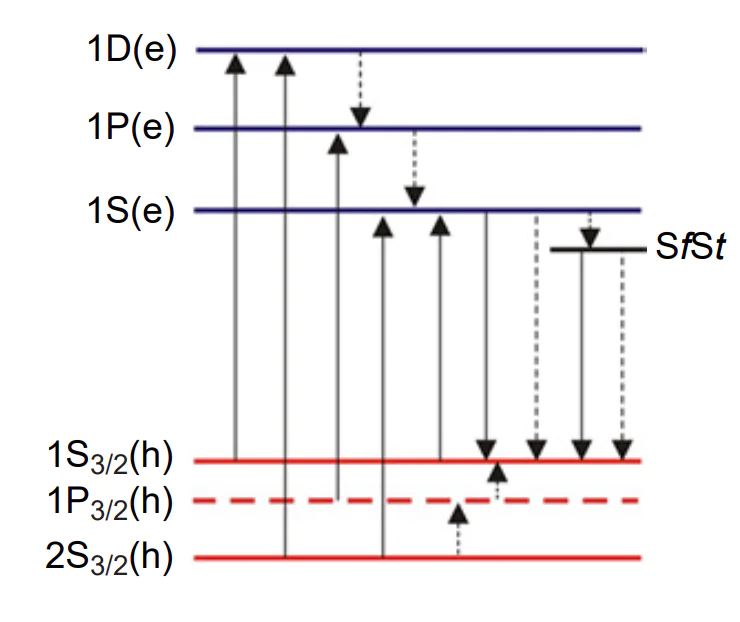
For the case of strong confinement in CdSe nanocrystals, inclusion of the effect of the Kane shape of the conduction band, degeneracy of the valence band consisting of light and heavy hole bands and split off band (Scheme 1) resulted in the energy structure shown in Figure 15a[111, 127]. In this case, the allowed optical transitions of noticeable intensity were as follows: 1S3/2(h) → Se, 2S3/2(h) → 1Se, 1S1/2(h) → 1Se, 2S1/2(h) → 1Se, 1P1/2(h) → 1Pe, 3S1/2(h) → 1Se, 2S3/2(h) → 2Se, 1P1/2so(h) → 1Pe and 4S3/2(h) → 2Se. The energy level diagram in semiconductor quantum dots based on direct band gap semiconductors is shown in Scheme 1, in which \( SfSt \) stands for the surface level (trap)[127].
![[{"id":"kxkWzw_u-v","type":"paragraph","data":{"text":"Energy level diagram for nanocrystals based on direct band gap semiconductors: (a) energy spectrum of electrons and holes depending on the squared average radius (\\( \\bar{a} \\)) of CdSe CQDs[[ type=\"anchor\" referenceId=\"2848\" ]]; (b) diagram of allowed energy transitions. The vertical dashed lines are non-radiative transitions[[ type=\"anchor\" referenceId=\"3946\" ]]."}}]](/storage/images/resized/EZ5drdNIlmWJXybXyfsgYsM1ISXVxrq8lI88mWIM_xl.webp)
In recent years, increasing attention has been paid to quantum dot structures based on indirect band gap semiconductors consisting of silicon, germanium, oxygen, hydrogen and carbon as they are less toxic than heavy elements such as Pb, Hg, Cd, etc. and, hence, suitable for medical applications. There is still no full understanding of the energy structure and mechanisms of radiative and non-radiative transitions in quantum dots.
Nevertheless, relying on the certain analogy between the luminescent properties of complex organic molecules in the condensed phase and the properties of quantum dot-based luminophores, an energy diagram for CQDs based on indirect band gap semiconductors has been proposed (Figure 16); the diagram consists of the singlet ground state (S0), first excited singlet state (S1) and metastable triplet state (Т1)[104, 127]. The transition between the Т1 and S1 states is forbidden by the spin selection rules. There are also high-lying singlet excited Sn (n > 1) and triplet Tn (n > 1) states. This diagram adequately describes the photophysical properties of quantum dot structures composed of indirect band gap semiconductors[127].
![[{"id":"vjx7WwsEf0","type":"paragraph","data":{"text":"Diagram of energy levels in indirect band gap semiconductor nanocrystals: (a) simplified energy diagram; (b) diagram[[ type=\"anchor\" referenceId=\"3946\" ]] of the allowed energy transitions. The vertical dashed lines are non-radiative transitions."}}]](/storage/images/resized/Yi1gHlGXYOpvF1d0iflXOFSNcCZ1u3AgXzWODb9w_xl.webp)
It is noteworthy that, unlike 2D-structures for photodetectors (e.g., QWIP, that is, numerous quantum wells grown by epitaxy), in which additional diffraction gratings, corrugated surfaces, island networks and so on must be used since optical transitions polarized in the photosensitive element (PSE) plane are forbidden, in the case of quasi-0D quantum dot structures, the absorption of photons upon normal incidence on the PSE surface is possible, since the above forbidding is removed[128]. This markedly decreases the complexity of the photosensitive structure and simplifies the production process.
4.2. Charge transport in CQD arrays
To attain a high quantum efficiency of photosensors based on quantum dots, it is necessary to generate a high concentration of charge carriers in CQDs. For this purpose, CQD ensembles (arrays) with a layer density of 1011 – 1012 cm–2 rather than single quantum dots should be used. The above description of the optical properties is generally valid for both single quantum dots and arrays. The presence of organic (e.g., oleic or mercaptopropionic acid residues, etc.) or inorganic ligands (e.g., I–, Cl– and so on) gives rise to only additional peaks (bands) in the absorption spectrum of the CQD array. However, analysis of the transport properties and charge transfer requires consideration of the whole set of nanocrystals that form the array. Although the properties of the array are still specified by the properties of constituent nanoparticles, the physical characteristics of the array may substantially differ from those of single CQDs. For example, a CQD array is characterized by a certain disorder, which is associated, in the simplest case, with different particle sizes and distances between the particles, different numbers of donors in each CQD, etc. As a result, the Fermi level position, dielectric permittivity, density of states and other characteristics may be considerably dissimilar for single quantum dots and for loose or dense CQD arrays.
Theoretical studies consider two types of structure for CQD arrays ordered to form a cubic lattice[129-131]:
(a) an array in which quantum dots are located at some distances from one another owing to ligands;
(b) quantum dots of the same size, but without ligands, which therefore touch one other with their faces.
Depending on the ratio between the dielectric permittivity values of single colloidal quantum dots (\( \varepsilon_{CQD} \)) and the medium in which the CQD array is immersed (\( \varepsilon_{i} \)) and the volume fraction \( f \) of quantum dots in the array, the dielectric permittivity of the array e is calculated by the relations presented in Table 2[130, 131], which considerably differ from the Maxwell – Garnett and Bruggeman equations derived in the framework of mean-field theory[129].
![Dielectric permittivity e of a quantum dot array for different ratios between the dielectric permittivity of a single CQD (eCQD), the medium in which the CQDs are immersed (ei) and the volume fraction of CQDs in the array (f). The Table was composed by the authors using published data[<a class="anchor" href="#reference-3952">130</a>, <a class="anchor" href="#reference-3953">131</a>].](/storage/images/resized/IY2OobE5JelTfWPPEPrd9rmv9DpzNlN4Y7cEsAHp_xl.webp)
The specific features of charge carrier transport across single quantum dots are related to the limited number of electrons located in the CQD energy level. When a quantum dot occurring in an electric field is located between two thin potential barriers, only charge carriers with a definite energy can be involved in the tunnelling current across the dot. If the tunnelling permeabilities of the barriers are different, electrons start to accumulate in the quantum dot and suppress the carrier transport across CQD due to their Coulomb potential (Coulomb blockade). Hence, an additional electron can be added to a CQD only provided that the energy of this electron is high enough to overcome the Coulomb blockade. In semiconductor CQDs, the kinetic energy of electrons is quantized due to the quantum confinement effect, and the quantization energy may far exceed the Coulomb blockade energy.
A theoretical description of the conduction mechanisms in quantum dot arrays was given by Reich[131]. Due to the Coulomb blockade effect noted above, the conductivity in an array of even metallic quantum dots decreases exponentially with temperature, i.e., such an array is usually a dielectric. Similarly, arrays of semiconductor quantum dots, including doped ones, are dielectrics, the conductivity of which is described by the formula[131]
in which coefficients \( E_0 \) and \( p \) depend on the conduction mechanism and temperature range.
The conduction mechanism in an array of doped quantum dots at low temperature usually corresponds to the Efros – Shklovskii model (\( \ln G \propto T^{-1/2} \)), the activation conduction mechanism (\( \ln G \propto T^{-1} \)) operates at high temperature, while in the intermediate temperature range, Mott transport is implemented (\( \ln G \propto T^{-1/4} \))[132]. For example, the Mott conduction mechanism is clearly manifested for CdSe CQDs in the 40 – 230 K temperature range (Figure 17a)[133].
Figure 17b,c present the temperature dependences of the conductivity in PbS CQD arrays[134]. In the temperature range of 25 – 220 K, two clear-cut activation conduction regions are observed (Figure 17b). In the (\( G \), \( T^{-0.25} \)) coordinates, the temperature dependence is less obvious (Figure 17c) and does not unambiguously attest to Mott conduction. The charge carrier transport in colloidal quantum dot arrays is addressed in a number of reviews[131, 135-137]. As opposed to metal nanoparticles, semiconductor CQDs are markedly affected by the quantum confinement, which accounts for a significant difference between the metal nanoparticle and semiconductor CQD arrays[135]. In the semiconductor CQD arrays, the disorder in the number of donors may lead to different numbers of electrons at different points. The effects of size, distance and donor number disorders on the conductivity of CQD arrays are considered in a review by Reich[131].
Organic semiconductors are characterized by strong disorder and weak interaction between molecules, which determines the hopping mechanism of charge carrier transport[138]. The same features of disorder associated with the scatter in size, number of donors and distances between the centres of nanocrystals are also characteristic of CQD arrays[131]. Therefore, charge carrier transport in CQD arrays can also occur via hopping between localized energy states of various nanocrystals[137].
The dynamics of intrinsic exciton diffusion in PbS CQDs was investigated by Zhang et al[139]. The authors observed a high exciton diffusion rate (~102 cm2 s–1) in PbS CQDs during the first several hundred femtoseconds after photoexcitation followed by relatively slow transport (~10–1 cm2 s–1). The authors attributed this fast transport to the large exciton Bohr radius, which is significantly larger than the CQD diameter. Layers with greater distances between CQDs have a higher initial diffusion rate and later transition to the slower transport stage (Figure 18)[139].
![[{"id":"LkBtpP3t8y","type":"paragraph","data":{"text":"Exciton transport in CQD layers with: (a) relatively long distance between quantum dots; (b) relatively short distance between CQDs[[ type=\"anchor\" referenceId=\"3962\" ]]."}}]](/storage/images/resized/HByNVeU2SCUQBRZx2D9YGevKcpprL2VF6HdQHJpF_xl.webp)
5. Single- and few-element photosensors based on CQDs
5.1. CQD materials for photosensors
Currently, colloidal quantum dots have been synthesized using quite a few semiconductors such as Si, graphite, graphene, ZnO, CdS, CdSe, CdTe, PbS, PbSe, PbTe, ZnSe, ZnS, ZnTe, Ag2Se, Ag2S, HgTe, HgS, HgSe, TiO2, InAs, InP, InSb, GaAs, GaN, GaP, GaInP2, CuInS2, CdxHg1–xTe, Zn(Te1–xSex), etc.
The development of high-temperature colloidal synthesis of quantum dots in 1993 opened prospects for the industrial production of a number of quasi-zero-dimensional materials with unusual and promising physical properties[37].
To date, a number of architectures of photosensitive elements based on both photoresistors and energy barrier structures formed by heterojunctions or CQD layers with electron and hole types of conduction have been studied[68, 140, 141]. The greatest success in the design of devices that were implemented in the commercial market of optoelectronics was achieved with the use of PbS CQDs. Apart from the mega-pixel (2.1 MP) cameras demonstrated in 2020 at an exhibition in the USA, a broad-band device based on PbS CQDs with pulse response time of < 3 ns was proposed in 2022[36].
Colloidal quantum dots based on compounds of other elements, AIVBVI and AIIBVI, are being actively studied. According to published data, the effective exciton Bohr radii in PbS, PbSe, PbTe, HgSe, HgTe and HgS are 18, 46, 150, 17, 40 and 50 nm, respectively[142-145]. The relatively large Bohr radius, together with the observed optical absorption (Figure 19)[146-151], makes these compounds promising for the development of near- and mid-wave IR devices. The following analysis of the architectures of CQD-based photosensitive elements will focus on colloidal quantum dots of lead and mercury chalcogenides (PbS, PbSe, HgTe, HgSe, HgS), which were used to fabricate various types of sensor elements.
5.2. Photoresistors
The size quantization in binary compounds of Group IV–VI elements was observed for ultrathin PbS and PbTe CQDs layers obtained by vacuum evaporation back in 1960[152]. Lead sulfide quantum dots synthesized as 8 – 30 nm nanocrystals inside a glass matrix by high-temperature heating of silicate glasses were described in 1994 by Borrelli and Smith[153]. In 2001, high-temperature colloidal synthesis of PbSe quantum dots was performed[154]. In 2003, a process for the fabrication of PbS-based colloidal quantum dots was described[155]. PbS and PbSe CQDs are self-assembled to ordered superlattices with high structure perfection and minimum size dispersion (<5%)[69].
The photoresistive structure studied by Hu et al.[156] was composed of a PbS CQD layer deposited onto interdigitated electrodes (Figure 20). Protection from the atmosphere was provided by a 30 nm-thick Al2O3 coating fabricated by atomic layer deposition (ALD) technique. Photosensitivity cut-off wavelength of 2.4 μm, responsivity of approximately 50 А W–1 (λ = 1.55 μm) and detectivity of 3.4 × 108 cm Hz1/2 W–1 at Т = 230 K were implemented.
![[{"id":"Y6gkoj6Vqf","type":"paragraph","data":{"text":"Photoresistive structure based on PbS CQDs with interdigitated finger electrodes. The Figure was created by the authors using published data[[ type=\"anchor\" referenceId=\"3978\" ]]."}}]](/storage/images/resized/wSKWOufG80ZFERdKLDvpReVL2zaFdVdSDo1lQP68_xl.webp)
The presence of ligands and dangling bonds on the CQD surface and the presence of surface oxygen adsorbents (such as PbSO3 PbSO4) gives rise to acceptor states in the band gap and finally results in the switching of the initially n-type PbS CQD layer to hole conduction with a concentration of ~1017 cm–3[157]. High concentration of the major charge carriers and the presence of traps for minor charge carriers in the band gap lead to high dark current density and low speed performance of photoresistors. Silver nanocrystals with low electron work function, being located in quantum dot layers near PbS nanocrystals, can act as a sort of donors by injecting electrons, which compensate the acceptor states and passivate the surface trap states. This is in sharp contrast to ionic doping, where replacement of lead cations gives rise to stronger p-type conduction in PbS nanocrystals. By mixing PbS CQDs and Ag nanocrystals in various ratios during the synthesis, the authors attained controlled doping of colloidal quantum dots where CQD layers switched to electronic conduction type[157]. The optimal PbS : Ag ratio was 1 : 0.05; in this case, \( D_{\lambda = 1.55}^* \) = 5 ×1011 cm Hz1/2 W–1 at λ = 1.55 μm and \( D_{\lambda = 0.6}^* \) = 1.2 × 1012 cm Hz1/2 W–1 at λ = 0.6 μm were attained (мкм надо заменить на μm). The frequency band amounted to 200 Hz. This method also leads to passivation of traps in the band gap. A CQD array can also be passivated by being coated with alumina[157].
Organic ligand shells can noticeably absorb IR radiation, thus limiting the spectral sensitivity range. The replacement of the oleate ligands in PbS CQDs by completely inorganic ligands provided a record-high long-wavelength operation of photoresistors (0.2 level at 3050 nm)[158]. The responsivity was 0.14 А W–1, the detectivity reached 1.1 × 1010 cm Hz1/2 W–1, and the frequency range was 3 kHz. A beneficial effect of ligand replacement was also noted by Konstantatos et al.[159, 160], who performed post-synthetic replacement of the oleate anion by n-butylamine and thus fabricated photoresistors with a specific detectivity D* of approximately 1013 cm Hz1/2 W–1 at room temperature. A noticeable result for PbS CQD photoresistors was attained by using completely inorganic As2S3 shells as stabilizers[161]. In the cited study, deposition of the absorbing film consisting of approximately 20 (NH4)3AsS3-coated PbS CQD layers on a glass substrate was followed by heating at 130 °С; as a result, the ligand was converted to a thin As2S3 layer transparent for IR radiation. In a PbS CQD – As2S3-based photoresistor (≈ 0.08 mm2 active area) with interdigitated Au electrodes (Figure 21)[161], the specific detectivity was 1.2 × 1013 cm Hz1/2 W–1 (λ = 1.3 μm) and the responsivity was 200 А W–1 (λ = 1.4 μm) at room temperature. The average size of the PbS colloidal quantum dots was 4.3 – 4.4 nm, which resulted in a relatively short cut-off wavelength λc ≈ 1.5 μm. He et al.[162] proposed a process for the formation of a photoresistive structure on a flexible substrate (paper-like material based on calcium carbonate and high-density polyethylene HDPE). A PbS CQD layer (the quantum dot diameter was 3.7 nm) was used as the photosensitive medium. Gold nanocrystals (8 nm in diameter) were introduced into the layer for doping and trap passivation, as described above for PbS CQD-based photoresistors with the addition of Ag nanocrystals. For a structure with an approximately 5% gold content, the specific detectivity was 1.1 × 1010 cm Hz1/2 W–1.
![[{"id":"N5qDeQPrnk","type":"paragraph","data":{"text":"PbS CQD-based photoresistor with the As<sub>2</sub>S<sub>3</sub> ligand: (a) photoresistor architecture; (b) spectral dependences of the absorbance of a PbS CQD:(NH<sub>4</sub>)<sub>3</sub>AsS<sub>3</sub> solution and a PbS CQD-As<sub>2</sub>S<sub>3</sub> film; (c) spectral dependence of the responsivity and detectivity at λ = 1.3 µm. The Figure was created by the authors using published data[[ type=\"anchor\" referenceId=\"3983\" ]]."}}]](/storage/images/resized/m0cd54R8Uot0T8SqPz6EMzHtbdm3EpI8Q6IVbyNc_xl.webp)
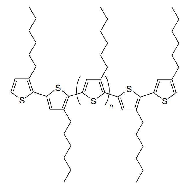
A number of publications address the properties of photoresistive structures based on PbSe CQDs[121, 163-168]. The PbSe@PbS core@shell heterophase nanostructures were reported by Sashchiuk and co-workers[164, 166]. The large exciton Bohr radius for bulk lead selenide (46 nm) promotes the formation of PbSe CQDs with a radius of more than 10 nm. The PbSe colloidal quantum dots obtained in 2001 by high-temperature colloidal synthesis at temperatures of 90 – 220 °С had diameters of 3.0 to 15.0 nm[121]. The range of optical absorption from 1.1 to 3.2 μm can be implemented in structures based on these quantum dots. Thambidurai et al.[167] reported photoresistors (Figure 22) manufactured using PbSe CQDs of ~8 nm in diameter perating up to 2.8 μm wavelength.
![[{"id":"QzQ1lgyzOS","type":"paragraph","data":{"text":"Photoresistor composed of PbSe CQDs with interdigitated electrodes: (a) photoresistor architecture; (b) spectral characteristic of the absorption of a CQD solution[[ type=\"anchor\" referenceId=\"3989\" ]]."}}]](/storage/images/resized/NVpcfsThi7RHcsh8jU7i1jdTH1w13Eu2WHP9qyxZ_xl.webp)
The responsivity, specific detectivity and quantum efficiency at an active layer thickness of 900 nm and at room temperature were 0.96 А W–1, 8.13 × 109 cm Hz1/2 W–1 and 78%, respectively[167]. Using lead stearate and a selenium solution in oleylamine (OLA – Se) as precursors, the authors synthesized PbSe nanocrystals of various shapes, including quasi-spherical, cubic, octahedral, cuboctahedral and star-shaped ones[163]. The nanocrystal size varied from 18.5 nm (quasi-spherical) to 46 nm (star-shaped).
The multiple exciton generation (MEG), that is, the formation of several excitons upon the absorption of one photon with the energy \( h\nu \gg E_g \), was found for the structures based on PbSe CQDs[169-171]. Owing to the multiple exciton generation effect, a quantum yield of 300% was attained for solar cells[170]. In 2008, the MEG effect was detected for PbS CQDs[172]. A review of studies dealing with MEG was reported in 2018 by Goodwin et al[173]. A paper by Jin et al.[174] addressed MEG in manganese-doped PbSe@CdSe core@shell structures.
Some studies note the high sensitivity of the PbSe CQD surface to the surrounding atmosphere, which requires surface stabilization and protection. The adverse effect of the atmosphere is usually attributed to the adsorption of oxygen, which increases the density of surface traps that impair the performance of photosensors. A number of publications describe the methods for stabilization using chlorination in the CQD synthesis and protection by using core@shell type heterostructures[166].
Several studies describe photoresistive structures based on HgTe and HgSe CQDs[117, 175-181]. Tang et al.[117] and Keuleyan et al.[175, 176] reported a process for the fabrication of a 12 × 12 mosaic array of photoresistors (Figure 23a). Each photoresistor in this two-dimensional array consists of three photosensitive elements with dimensions of approximately 220 × 220 μm attached to interdigitated electrodes (Au/Cr) for supplying power voltage and recording the photosignals (Figure 23b). Each of the three photosensitive elements is a HgTe CQD layer with a small, medium or relatively large diameter and thickness of 410, 340 or 210 nm deposited on top of the interdigitated electrodes (Figure 23c). Figure 23d shows the spectral dependences of absorbance of HgTe CQDs with different quantum dot diameters. The cut-off wavelength of the photoresistor with a CQD layer of 20 nm was approximately 9.5 μm. The selected CQD sizes provided cut-off wavelengths for the three-element photoresistors of λc1 ≈ 4.8 μm, λc2 ≈ 6.0 μm and λc3 ≈ 9.9 μm[177].117 The maximum responsivity was approximately 0.1 А W–1 and the specific detectivity was about 2 × 107 cm Hz1/2 W–1. These studies demonstrated the possibility of fabricating multiple-spectrum photosensors based on colloidal quantum dots sensitive in the short-wave, mid- and far-infrared ranges.
![[{"id":"e4YtMpCpAw","type":"paragraph","data":{"text":"Three-spectrum mosaic photoresistor arrays based on HgTe CQDs: (a) external view of the product (12×12 array); (b) diagram of interdigitated metal electrodes (Au/Cr) on SiO<sub>2</sub>/Si substrate; (c) three-electrode photoresistor based on colloidal quantum dots of three different diameters deposited onto metal electrodes; (d) spectral dependences of the absorbance of HgTe CQDs of 6, 11, 15 and 20 nm in diameter[[ type=\"anchor\" referenceId=\"3938\" ]]."}}]](/storage/images/resized/kxIwcbB6OMNNlEjVkHufaRvsRYLNNMpE4vF7ERQR_xl.webp)
Tang et al.[117] investigated photosensors based on HgSe CQDs. Photosensors with the structure depicted in Figure 24a represented photoresistors fabricated on the SiO2/Si chip. The photoconductivity was due to 1Se → 1Pe intraband transitions. The size of colloidal quantum dots determining the spectral sensitivity range was ~5 to ~16 nm and was specified by the synthesis temperature and time. The photosensitivity was implemented over a wide wavelength range. The centre wavelengths for the four studied photoresistors were λmax1 = 4.2 μm, λmax2 = 6.4 μm, λmax3 = 7.2 μm and λmax4 = 9.0 μm (Figure 24b). The high-resolution transmission electron microscopy (TEM) image of HgSe CQDs is shown in Figure 24c. For increasing the optical absorption, the authors used plasmonic antennas, which were designed as metal nanodisks, with their size and distance between them being specified depending on the size of quantum dots and absorbed wavelength. The nanodisks were made of 80 nm-thick gold layers and coated with approximately 10 nm-thick SiO2 layers. For λmax1 = 4.2 μm, the plasmonic disk diameter was D = 1000 nm, while the distance Р between the centres of the disks on the SiO2 film coating the Si substrate was chosen to be equal to 2D (Figure 24d). The responsivities for the elements characterized by the centre wavelengths were 145, 92.3, 88.6 and 86.0 mA W–1.
![[{"id":"y9uz5fAy3A","type":"paragraph","data":{"text":"Photoresistor based on HgSe CQDs with plasmonic Au nanodisks: (a) photoresistor architecture; (b) spectral dependences of the responsivity of CQDs of different diameters (~5 to ~16 nm); (c) TEM image of CQDs; (d) SEM image of plasmonic disks of 1000 nm in diameter with a 2000 nm distance between the centres on the SiO<sub>2</sub> surface[[ type=\"anchor\" referenceId=\"3999\" ]]."}}]](/storage/images/resized/V56IbpZce0AnB6U9pgF2BtxJVi1nSIJE8RratQZo_xl.webp)
The key characteristics of few-element photoresistive structures based on PbS, PbSe, HgTe and HgSe CQDs are presented in Table 3[177, 156-163, 179-182].
5.3. Photosensors with energy barriers
This Section addresses heterosystems consisting of several contacting solid phases composed of colloidal quantum dot arrays with different band gaps or arrays of identical CQDs but characterized by different types of conduction in different parts of the heterosystem. In all cases, these heterophase photosensors have one or more energy barriers, which provide effective separation of charge carriers formed upon the decay of excitons generated by the absorbed radiation. The energy barriers of photosensors may be based on various types of heterojunctions (P-n, N-p, P-p, n-N), Schottky barriers, p-i-n homo- and heterojunctions, bariode heterosystems, etc. Most of modern photosensor arrays made of traditional 3D semiconductors are based on the same principles.
Photovoltaic sensors for measuring IR radiation that are being developed or have been developed to date using CQDs can be conventionally assigned to one of the following types: Schottky photodiodes, p-n junction structures, p-i-n structures, transistor structures and heterojunction structures of various types. Analysis of the available literature devoted to this subject indicates that various organic and nanocomposite materials consisting of a conductive organic polymer and inorganic nanoparticle are widely used in these designs (for example[183]). The range of organic compounds applied in this area is very broad and is largely inherited from solar cell and organic light-emitting diode technologies. In the beginning of the 21st century science and engineering areas called ‘organic photonics’ and ‘organic optoelectronics’ appeared in optoelectronics[184, 185].
Tang et al.[70] studied a photodiode structure with a Schottky barrier at the HgTe CQD/Au contact (where Au acts as the top contact) (Figure 25a). The bottom contact was made of ~30 nm-thick ITO layer, on which Au plasmonic disks were deposited. The most pronounced plasmon resonance in the described structure was attained in the case of 350 nm diameter of plasmonic disks and approximately 700 nm distance between their centres. The optical absorption curves in the 1.7 – 5 μm wavelength range are shown in Figure 25b and demonstrate the effect of plasmon resonance and the optical interference device located in the upper part of the structure on the absorbance. The highest responsivity reached 1.62 А W–1 (Figure 25c), which corresponds to quantum efficiency of 45%. The presence of plasmonic disks increased the specific detectivity from 1.2 × 10¹¹ to 4 × 1011 cm Hz1/2 W–1 at Т = 85 K and from 3.1 × 10⁸ to 7.2 × 108 cm Hz1/2 W–1 at Т = 295 K. At the temperature Т = 220 K, which can be attained using a thermoelectric cooler, a specific detectivity of 1 × 1010 cm Hz1/2 W–1 can be reached (Figure 25d). The effect of plasmon resonance and interference devices on the current – voltage characteristic of the photodiode structure is depicted in Figure 25e.
![[{"id":"IC1oPa5OSk","type":"paragraph","data":{"text":"Photodiode sensor with a Schottky energy barrier based on HgTe CQDs with plasmonic disks and interference device: (a) photosensor architecture; (b) absorption curves in the presence (continuous line) and in the absence of plasmonic disks and interference device (dashed line); (c) spectral sensitivity of the photosensor in the presence of plasmonic disks and interference device; (d) temperature dependence of the detectivity under illumination from a black body (BB) at Т<sub>BB</sub> = 600 °С and modulation frequency of 500 Hz; (e) CVC of the photodiode structure under illumination from a BB at Т<sub>BB</sub> = 600 °С (curves 2 and 3) and without illumination (curve 1) in the presence (curve 3) or in the absence (curve 2) of plasmonic disks and interference device; the dashed line in Figures (b, c) shows dependence of the absorbance and sensitivity on the wavelength without plasmonic disks and interference device[[ type=\"anchor\" referenceId=\"3894\" ]]."}}]](/storage/images/resized/GO0QHdcku6gjsXBjKVVGuN0M5wHZziPaK6AHPEBq_xl.webp)
Subsequently, a few more structures of photovoltaic sensors based on HgTe CQDs with a Schottky barrier have been proposed and studied. Jagtap et al.[186] described a Schottky photodiode with the glass/ITO/TiO2 CQDs/HgTe CQDs/Au structure (Figure 26a) and sensitivity up to λc ≈ 2.5 μm (4000 cm–1). Owing to the electron type of conduction of titanium dioxide, the barrier at the TiO2/HgTe CQDs interface prevents the passage of photoholes, thus reducing the dark current. The current – voltage characteristic of the photodiode structure is shown in Figure 26b. The specific detectivity at room temperature was 1.5 × 107 cm Hz1/2 W–1.
![[{"id":"Cfxrq5nWCL","type":"paragraph","data":{"text":"Schottky barrier photodiode with the glass/ITO/TiO<sub>2</sub> CQDs/HgTe CQDs/Au structure (a) SEM image of the structure cross-section; (b) photodiode CVC[[ type=\"anchor\" referenceId=\"4007\" ]]."}}]](/storage/images/resized/wG7mR3HJjd0qXVuGPcfit5vWgfXD5Ojp99iWSvRY_xl.webp)
The subsequent advancement of HgTe CQD photodiodes is associated with the development of ways to expand the spectral sensitivity range and reduce dark currents, which noticeably reduce the detectivity, by incorporating energy barriers similar to the blocking barriers in bariode heterosystems XBnn and XBpp, capable of suppressing the dark injection of electrons and holes[187]. This photosensor for recording the IR radiation at λ > 2 μm has the structure: substrate/ITO or FTO/TiO2 CQDs/i-HgTe CQDs/p-HgTe CQDs/MoO3/Au (Figure 27a), where FTO is fluorine-doped tin oxide[188, 189]. The radiation is absorbed in the HgTe CQD layer with ambipolar conduction (λc = 2.9 μm). CQDs with cut-off wavelengths λc of 6000 cm–1 (1.67 μm), 4000 (2.5 μm) and 700 cm–1 (14.3 μm) have the hole, ambipolar and degenerate electron types of conduction, respectively[188]. The TiO2 layer suppresses the dark current of holes from the ITO (or FTO) layer, while p-type HgTe CQD and MoO3 layers block the dark electron current from the gold contact (Figure 27b). A specific detectivity of 3 × 108 cm Hz1/2 W–1 (Figure 27c) at Т = 300 K was implemented in the structure.
![[{"id":"0os9f2I3Pm","type":"paragraph","data":{"text":"Photodiode with a unipolar energy barrier at the TiO<sub>2</sub>/HgTe CQD contact with unipolar conduction and an additional barrier at the MoO<sub>3</sub>/Au contact: (a) photodiode structure; (b) energy diagram of the structure; (c) specific detectivity: (1) for the photosensor shown in Fig. 27a, (2) for the photosensor shown in Fig. 26a[[ type=\"anchor\" referenceId=\"4009,4010\" ]]. PVA is poly(vinyl acetate), PMMA is poly(methyl methacrylate)."}}]](/storage/images/resized/0xwvn3P2XMkta14m0Gxp3lGYkEfGEMujdj6naRDM_xl.webp)
A photosensor based on the HgTe CQDs : HgSe CQDs mixture with random distribution of CQDs in the layer was proposed in 2019 (Figure 28a)[190]. An energy structure (Figure 28b) similar to the structure of multiple quantum wells in GaAs/AlGaAs-based QWIP (Figure 28c) is formed in this case in the CQD nanolayer. The photosensor is a photodiode structure in which the illumination is performed through a thin (80 nm) aluminium electrode with 70% optical transmittance in the mid-IR region. The HgTe nanocrystals provide the formation of an energy barrier (analogues of AlGaAs in QWIP), while HgSe nanocrystals are responsible for the appearance of energy wells (analogue of GaAs in QWIP). Thus, the device combines the intraband absorption via 1Se → 1Pe transitions in HgSe CQDs and the transport of photocarriers over barriers formed by HgTe CQDs (the mobility is higher in HgTe than in HgSe). The optical and transport properties of the quantum dot layer consisting of the HgTe CQD : HgSe CQD mixture depends on the dot size and the relative content of HgSe in the HgTe matrix. FFigure 28d shows the photosensitivity spectrum for several HgTe CQD : HgSe CQD mixtures with different contents of HgSe (the HgTe CQD matrix consists of quantum dots with a diameter providing the cut-off wavelength λc ≈ 2.5 μm). The photoresponse relaxation time shown in Figure 28e (measured for field-effect transistor samples with channels made of HgTe CQD : HgSe CQD mixtures) is approximately 1 ms when the HgSe fraction is high and decreases below 100 μs with increasing HgTe fraction. By reducing the fraction of HgSe CQDs from 100% to 18%, it is possible to increase the effective energy barrier width [i.e., the average distance \( \Delta L \) (Figure 28b) between nanocrystals in the HgSe : HgTe layer] from ~1 to ~60 nm. The responsivity of the photodiode structure upon illumination from BB with 1.9 μm high-pass filter is a few mA W–1. The noise is defined as 1/f. The specific detectivity at Т = 80 K and modulation frequency of 1 kHz was \( D_{BB}^* \cong \) 1.5 · 109 cm Hz0.5 W–1. The current – voltage characteristics of the photodiode structure are depicted in Figure 28f.
![[{"id":"LePgvoTk1N","type":"paragraph","data":{"text":"Structure and characteristics of the photosensor based on the HgSe CQD:HgTe CQD mixture: (a) photosensor structure; (b) energy diagram of the photosensor based on the HgSe CQD:HgTe CQD mixture; (c) energy diagram of the QWIP photosensor based on GaAs/AlGaAs; (d) absorption spectrum of nanolayers consisting of a HgSe CQD:HgTe CQD mixture with different contents of HgSe and HgTe at a HgTe CQD diameter providing a cut-off wavelength of 2.5 µm; (e) photoresponse relaxation time for different contents of HgSe at Т = 200 K; (f) current–voltage characteristics of the photodiode structure at Т = 80 K, (1) under illumination at \\( \\lambda \\cong \\) 4.4 µm, (2) without illumination[[ type=\"anchor\" referenceId=\"4011\" ]]."}}]](/storage/images/resized/hMyxumz8VpUfNKS9Cc6gm8OQlFpD5MGzupv55qI0_xl.webp)
In 2019, X.Tang et al.[191] developed and studied the architecture of a dual-band photosensor for the 1.5 – 2.5 μm (SWIR) and 3 – 5 μm (MWIR) spectral ranges consisting of two photodiodes based on colloidal quantum dots combined into one n-p-n structure (Figure 29a). SWIR radiation is absorbed by the top photodiode consisting of HgTe CQDs of 6 nm in diameter. The MWIR radiation is absorbed in the bottom layer consisting of HgTe CQDs of 9 nm in diameter. The 5 nm-thick semi-transparent Au top electrode transmits ~60% of incident IR radiation. The bottom electrode is fabricated of ITO layer deposited on the Al2O3 substrate. Switching from one band to another is performed by changing the polarity of voltage applied to the structure. The n- and p-regions of the photodiode are generated using doped Bi2Se3 CQD and Ag2Te CQD layers, which serve as sources of donor and acceptor impurities in the HgTe CQD layers.
![[{"id":"f8IXL7Ni1A","type":"paragraph","data":{"text":"Dual-band photosensor based on CQD photodiodes combined into a single n-p-n structure: (a) photosensor structure; (b) energy diagram; (c) temperature dependences of the specific detectivity for SWIR and MWIR photodiodes forming the dual-band photosensor; (d) spectral dependences of the photoresponse at different bias voltages applied to the photosensor; (e) photosensor CVC[[ type=\"anchor\" referenceId=\"4012\" ]]."}}]](/storage/images/resized/28tHmPBDaTPdUGKcfY17loqwmu6O8Orfc645PlOb_xl.webp)
The diffusion of Ag+ ions gives rise to the acceptor р layer, whereas the n-layer is formed due to the charge transfer from the Bi2Se3 phase to HgTe. The energy diagram of the photosensor structure is shown in Figure 29b. The specific detectivity of the SWIR photodiode in the presence of the Bi2Se3 n-layer reaches 6 × 1010 cm Hz1/2 W–1 at room temperature and increases to 1 × 1011 cm Hz1/2 W–1 on cooling to 200 K (Figure 29c). The spectral dependences of the photosensitivity and CVC of photodiodes are shown in Figure 29d,e.
By 2023, the detectivity of photodiodes based on HgTe CQDs reached 1 × 1011 cm Hz1/2 W–1 at room temperature (λ = 2.2 μm, Т = 300 K)[192] and approximately 1 × 1010 cm Hz1/2 W–1 at low temperature (λ = 4 – 5 μm, Т = 200 K)[193]. With an appropriate selection of ligands, the responsivity Si and charge carrier mobilities me and mh at room temperature were Si = 0.23 А W–1, me = 3.4 cm2 × V–1 × s–1 and μh = 0.45 cm2 × М–1 × s–1[194]. The use of plasmonic structures to enhance optical absorption provided an increase in Si to approximately 1.6 A W–1[70].
The highest reported parameters of photosensors based on HgTe CQD photodiodes with a dot gradient homojunction were described by Xue et al[195]. At λ = 4.2 μm and 80 K, the specific detectivity and responsivity were D* = 2.7 × 1011 cm Hz1/2 W–1 (Figure 30c) and 2.7 А W–1, respectively, and the quantum efficiency reached 77%[195]. Note that the detectivity of photodiodes operating in the background limited infrared photodetector (BLIP) mode does not exceed \( D_{\lambda = 4.2 \mu m}^* \) (BLIP, Tbackground = 300 K, θ = 2π, f = 100 Hz is the radiation modulation frequency) \( \cong \) 3 × 1011 cm Hz1/2 W–1[4]. Thus, the described photosensor based on HgTe CQDs[195] actually has the highest possible detectivity for photodiode structures in the mid-wave IR range. The indicated result for HgTe CQDs was implemented owing to the original architecture (dot gradient homojunction) proposed earlier by Xue et al[195]. (Figure 30a,b) for a PbS CQD-based photodetector[195]. A three-stage procedure of primary ligand replacement modified by the authors was also used to implement the photosensor architecture Au/p-HgTe CQDs/p–-HgTe CQDs/i-HgTe CQDs/n–-HgTe CQDs/n-HgTe CQDs/ITO/sapphire and provided high charge carrier mobility in the HgTe CQD layer, exceeding 1 cm2 V–1 s–1.
![[{"id":"SO9c9dsOg9","type":"paragraph","data":{"text":"Photosensor based on HgTe CQDs with a dot gradient homojunction: (a) architecture; (b) energy diagram; (c) spectral dependence of the specific detectivity of photosensors the architecture of which involves p-i, i-n and p-i-n energy barriers[[ type=\"anchor\" referenceId=\"4016\" ]]."}}]](/storage/images/resized/l7k7KyAy2h3sBIiXBFvSAsaBHEc3mmFsxSqRnOHA_xl.webp)
Photovoltaic sensors based on CQDs of binary compounds of AIV and BVI elements were designed with Schottky barriers at the CQDs/metal contact, various heterostructures including polymer materials and 2D elements, and barriers at the contact between p- and n-type CQD layers.
Clifford et al.[196, 197] studied a SWIR photosensor with a Schottky barrier with the Al/PbS CQD/ITO/glass substrate structure (Figure 31)[183, 196-198]. The quantum dot absorption layer with a thickness of approximately 100 – 300 nm consisted of PbS nanocrystals of ~6 nm in diameter.196, 197 The Schottky barrier was formed at the contact between PbS CQD and a 100 nm-thick aluminium layer (3.14 mm2 area) fabricated by thermal deposition. The effective band gap in the semiconductor quantum dots (the distance between the 1Se and 1Sh levels) amounted to 0.86 eV, which is close to the value found from the relation Eg = 0.41 + (0.0392 D2 + 0.114 D)–1 (where D is the CQD diameter). The following photodetector characteristics were attained: spectral sensitivity range of 0.4 – 1.8 μm, quantum efficiency ≈17% (λ = 1.55 μm), specific detectivity D* = 1.5 × 1012 cm Hz1/2 W–1 (λ = 1.12 μm, Т = 250 K), D* = 0.7 × 1012 cm Hz1/2 W–1 (λ = 1.12 μm, Т = 300 K), D* = 0.4 × 1012 cm Hz1/2 W–1 (λ = 1.6 μm, Т = 250 K) and D* = 0.8 × 1012 cm Hz1/2 W–1 (λ = 1.45 μm, Т = 300 K) and transmission band width >2.9 МHz[197, 198].
![[{"id":"q6_zvoTSEg","type":"paragraph","data":{"text":"Photodetector with the Schottky barrier at the Al/PbS CQDs/ITO/glass substrate: (a) photodetector architecture[[ type=\"anchor\" referenceId=\"4018\" ]]; (b) spectral dependence of the quantum efficiency at Т = 295 K and specific detectivity at Т = 250 K[[ type=\"anchor\" referenceId=\"4019\" ]]; (c) temperature dependences of specific detectivity[[ type=\"anchor\" referenceId=\"4019\" ]]; (d) diagram of addition of Schottky photodiodes to the readout integrated circuit[[ type=\"anchor\" referenceId=\"4005\" ]]; (e) energy diagram of the structure, where \\( E_F \\) is the Fermi level, \\( q \\) is the charge of the electron, \\( F_b \\) is the height of Schottky barrier, \\( V_{bi} \\) is the built-in potential, \\( V_{int} \\) is the potential drop near the barrier[[ type=\"anchor\" referenceId=\"4017\" ]]; (f) current–voltage characteristics of the Schottky diode at various temperatures[[ type=\"anchor\" referenceId=\"4017\" ]]."}}]](/storage/images/resized/PYdIMdYs528wTcu5iQTBoIcDhJhV3mEKGCDXOVT4_xl.webp)
The relatively low quantum efficiency in Schottky barrier structures in the wavelength range λ > 1.2 μm (~17%) stimulated the development of photosensitive elements based on PbS CQDs and heterojunction structures using organic polymers.
The architecture of a photosensor with a bulk heterojunction and the active layer made of the PbS CQD : PCBM : P3HT : ZnO CQD mixture for the 0.3 – 1.1 μm range is shown in Figure 32a[199]. The average size of PbS CQDs and ZnO CQDs is 3.3 – 3.7 nm and 5.0 nm, respectively. Initially, two mixtures, PbS CQD : PCBM : P3HT and ZnO CQD : PCBM : P3HT, were prepared; then they were mixed to form a four-component mixture. The thickness of the active layer was 200 – 300 nm. The spectral dependence of the sensor photosensitivity is shown in Figure 32b. Due to the presence of ZnO CQDs in the active layer, the short-wave sensitivity extends up to the UV region. In the absence of illumination, this structure behaves as a photodiode, while under illumination, ohmic conduction is observed. The spectral characteristics of the detectivity for this structure is shown in Figure 32c.
![[{"id":"cyHBYGB4bD","type":"paragraph","data":{"text":"Photovoltaic cell with active absorption region based on the PbS CQD:PCBM:P3HT:ZnO CQD mixture with bulk heterojunction: (a) cell architecture; spectral dependences of the (b) absorbance and (c) specific detectivity[[ type=\"anchor\" referenceId=\"4020\" ]]."}}]](/storage/images/resized/3ZlNaEtvFR4oQ6gaEJRAjJn88ZkR2oaVwnDNygry_xl.webp)
SWIR photodetectors fabricated as Al/ZnO NPs/PbS@CdS/P3HT/PEDOT : PSS/ITO structures with the active absorption layer based on core@shell quantum dots, with the core consisting of PbS nanocrystals and the shell being made of CdS (λc ≈ 1.45 μm, and the first exciton absorption peak is located at 1.41 μm), were studied by Kwon et al[200]. By varying the core and shell materials, one can deliberately control the properties of the structure, where the core determines the absorption spectrum and the shell provides passivation of the core surface and low recombination of charge photocarriers. The average size of PbS colloidal quantum dots used to manufacture these photodetectors was in the 4.6 – 5.6 nm range, and the active absorption layer area was 9 mm2. The attained responsivity was 600 А W–1, while the specific detectivity was very high, 7.4 × 1012 cm Hz1/2 W–1. High characteristics of the photovoltaic solar cells based on core@shell quantum dots made of various materials were noted by Selopal et al.[201], who demonstrated good prospects of using these structures in photosensorics.
Due to the relatively high bond energies in organic materials, the photogenerated excitons dissociate slowly, thus deteriorating the photosensor performance. The use of PbS CQDs, the size of which is controlled by varying the conditions of synthesis, makes it possible to form a heterojunction providing an efficient separation of electrons and holes formed upon the photoexciton dissociation. The architecture of this photosensor is fabricated by deposition of a film made of a mixture of organic materials on the PbS CQD layer[202]. The average size of PbS CQDs used in the cited study is 3 nm; the first exciton absorption peak is located at 0.77 μm. After replacement of the oleate anion used in the PbS CQD synthesis by the iodide anion by treatment CQDs with tetra-n-butylammonium iodide (TBAI), the exciton absorption peak shifts to 0.83 μm. The organic polymer PBDB-T mixed with polyimidazoleporphyrin PBI-Por was used as the second layer deposited on top of the PbS CQD-TBAI layer.
The photosensitive element had the structure Al/ PBDB-T : PBI-Por/PbS CQD-TBAI/PBDB-T : PBI-Por/Al. The specific detectivity at 0.63 μm was 1.12 × 1013 cm Hz1/2 W–1. The photosensors with sharply unsymmetrical energy barriers at the n-ZnO/p-PbS CQDs and n-TiO2/p-PbS CQDs contacts in Al/n-ZnO/p-PbS CQDs/PEDOT : PSS/ITO and Au/p-PbS CQDs/n-TiO2/ITO structures, characterized by a quantum efficiency of approximately 70 – 80% (λ = 0.5 – 0.6 μm), were studied by Pal et al[203].
Due to the large surface area to volume ratio of PbS CQDs, the surface atoms can strongly affect the conductivity and charge carrier mobility in the layers of colloidal quantum dots. Thus, by selecting the appropriate ligand, it is possible to control, within certain limits, the energy levels of the conduction band minimum (CBM), valence band maximum (VBM) and the Fermi level (EF) in the CQD layer. Figure 33a shows the VBM, CBM and EF energy levels for PbS CQDs with various ligands such as benzene-1,2-dithiol (1,2-BDT), benzene-1,3-dithiol (1,3-BDT), benzenethiol (BT), ethane-1,2-dithiol (EDT), 3-mercapto-propionic acid (MPA), ethylene-1,2-diamine (EDA), ammonium thiocyanate, tetra-n-butylammonium halides [tetra-n-butyl-ammonium fluoride, TBAF; tetra-n-butylammonium chloride, TBACl; tetra-n-butylammonium iodide, TBAI], etc. (Scheme 2)[204]. In the case of 1,3-BDT ligand, the Fermi level in the PbS CQD layer occurs near the centre of the band gap, thus providing a conduction mechanism close to the intrinsic conduction. Using this ligand, Lee et al.[205] designed a p-i-n SWIR photosensor with i-type PbS CQDs. The photodetector had the structure Ag/MoO3/p-TAPC/i-PbS CQDs/n-ZnO/ITO/ glass substrate (Figure 33b) in which the p-TAPC {1,1-bis[4-(ditolylamino)phenyl]cyclohexane} layer is known as an effective material for hole transport and blocking of the electron current. The n-ZnO layer forms a barrier that blocks the hole current. The MoO3 layer serves for the transport of holes (extraction of minor carriers from the region in contact with the metal). The p-TAPC and n-ZnO blocking layers decrease the dark current density and provide specific detectivity of approximately 7 × 1013 cm Hz1/2 W–1 (λ = 1.23 μm) at room temperature (Figure 33c).
![[{"id":"ZAGXQ1Lw8h","type":"paragraph","data":{"text":"(a) Energy diagrams of the PbS CQD layer with various ligands, with the first exciton absorption peak before replacement of oleic acid by an appropriate ligand being at λ = 963 nm in the absorption spectrum of the solution. Each level in the Figure was determined by measuring 2–4 samples; the line width is the deviation from the mean value[[ type=\"anchor\" referenceId=\"4025\" ]]. (b) Architecture of p-i-n photosensor. (c) Spectral dependence of the specific detectivity[[ type=\"anchor\" referenceId=\"4026\" ]]."}}]](/storage/images/resized/XIaBOV70E9h5gXIVl9EslDd67iqCSSx2h4SFber5_xl.webp)
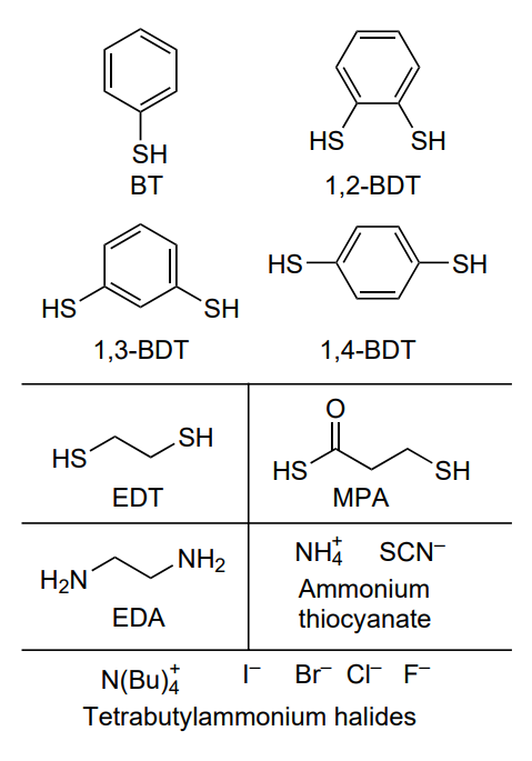
In recent publications, owing to relatively short molecular chains and high affinity to cations on the PbS CQD surface, EDT and TBAI have been more and more often used as ligands in the fabrication of quantum dot layers for solar cells and photosensors[206, 207]. A PbS CQD array passivated by EDT acquires p-type conduction. The PbS CQD array with the TBAI ligand has a clear-cut electron conduction (n-type), owing to the replacement of divalent S2– anions by I–.
In PbS CQD arrays, iodine-containing ligands protect lead sulfide nanocrystals from oxidation[208, 209]. Skurlov et al.[207] investigated the properties of PbS CQD arrays passivated by NH4I, PbI2 and (Bu)4NI. Recently, the development of these techniques led to the design of a new type of photodiode structures with an energy barrier at the p-PbS CQD-EDT/n-PbS CQD-TBAI contact. The architecture of these photosensors is depicted in Figure 34a,b[208-210]. For optimal layer thicknesses of 40 and 160 nm for p-PbS CQD-EDT and n-PbS CQD-TBAI, respectively, the photodiode Au/p-PbS CQD-EDT/n-PbS CQD-TBAI/ZnO/ITO was characterized by specific detectivity of 3.93 × 1013 cm Hz1/2 W–1 (λ = 0.91 μm) and 4.52 × 1013 cm Hz1/2 W–1 (λ = 0.5 μm) at room temperature under reverse bias of 0.04 V[208]. The responsivity was 385 А W–1 (λ = 0.91 μm) and 444 А W–1 (λ = 0.5 μm). Zinc oxide acted as a barrier blocking the hole current towards the ITO contact, while the p-PbS CQD-EDT layer blocked the electron current towards the Au contact. Photons were mainly absorbed in the n-PbS CQD-TBAI layer.
![[{"id":"YMza7LKXOb","type":"paragraph","data":{"text":"Characteristics of the photosensor Au/p-PbS CQD-EDT/n-PbS CQD-TBAI/ZnO/ITO: (a) architecture; (b) SEM image of the cross-section; (c) energy diagram of the heterojunction; (d) spectral dependence of absorbance; (e) CVC of heterostructure under illumination at 0.91 µm (2.0 µW cm<sup>–2</sup>) and without illumination[[ type=\"anchor\" referenceId=\"4029\" ]]."}}]](/storage/images/resized/rNBd07Wv6PjGLv66WvSzHO8qUztvOnpVn6kzFemq_xl.webp)
The architecture of a photosensitive element based on PbS colloidal quantum dots, AgNW/p-PbS CQD-EDT/n-PbS CQD-TBAI/Ni/Cr, where NW is nanowire, is shown in Figure 35a[211]. For the fabrication of the n-type PbS CQD layer, the initial ligand (oleate anion) used in the synthesis was replaced by a iodide anion by treatment with TBAI. The p-type conduction was generated by replacing the initial ligand by EDT. Lead chloride (PbCl2) was used as lead precursor and N,N'-diphenylthiourea [SC(NHPh)2] served as the sulfur precursor. The CQD size (7.6 nm) in the PbS CQD-TBAI(n) layer was greater than the CQD size (3.1 nm) in the PbS CQD-EDT(p) layer, which provided an additional energy barrier between the n- and p-type conduction layers due to different band gap widths and was achieved by varying the synthesis temperature. The n-ZnO nanoparticles of 7 – 8 nm size were synthesized by the method described by Beek et al[212]. As opposed to the studies cited above, the top IR-transparent anode layer was formed by aerosol printing from silver nanowires (AgNWs). They have optical transmittance of about 85 – 90% in the visible and short-wave IR regions, while having a sufficiently high conductivity, reaching 20 – 40 Ω m–1[213]. Thus, all functional layers (n-ZnO, n-PbS CQD-TBAI, p-PbS CQD-EDT, anode) were fabricated by liquid colloidal chemistry methods without the use of vacuum or high-temperature processes. The fabricated photosensitive elements had 12 × 12 μm size. The current – voltage characteristics of the photosensitive elements under illumination (light) or without illumination (dark) are shown in Figure 35b. The differential resistance of the dark CVC at zero bias for the studied samples is in the range of (2 – 20) × 1010 Ω. The breakdown voltage for various samples is approximately 1.7 – 2.0 V. The spectral dependence of the relative photosensitivity Si(l)/Si(lmax) is depicted in Figure 35c (curve 1), together with that for a sample of the previously described barrier structure based on PbS colloidal quantum dots (curve 2)[76]. The average relative spectral sensitivity Si(l)/Si(lmax) in the wavelength range of 0.9 – 1.85 μm for the sample studied by Popov et al.[211] was 1.5 times as high as that reported previously[76] for PbS CQD barrier nanostructures.
![[{"id":"0jJx8kRvvN","type":"paragraph","data":{"text":"Characteristics of the photosensitive element AgNW/p-PbS CQD-EDT/n-PbS CQD-TBAI/Ni/Cr[[ type=\"anchor\" referenceId=\"4032\" ]]: (a) architecture; (b) CVC under illumination with an electric filament lamp, incident power of ~3 mW, and without illumination; (c) spectral dependence of the relative photosensitivity for (1) the sensor architecture shown in inset[[ type=\"anchor\" referenceId=\"4032\" ]] (a) and (2) the PbS/C<sub>60</sub> architecture on the ROIC surface[[ type=\"anchor\" referenceId=\"3900\" ]]."}}]](/storage/images/resized/k6IaDUsHfhUkuAMYaXJAYTTdSqk2B1oCUKH5LN6u_xl.webp)
The properties of Ag/CsPbBr3 CQDs/PbSe CQDs/Ag and Au/ PbSe CQDs/CdS/CdSe : In/Si heterostructures are presented in Table 4[36, 70, 76, 191, 192, 195, 197, 199, 200, 202, 205, 214, 215].
The photosensors with and energy barrier at the contact between two arrays of different colloidal quantum dots of mercury and silver tellurides (HgTe CQDs and Ag2Te CQDs) with the sapphire/ITO/HgTe CQD/p-Ag2Te NP/Au architecture were studied by Ackerman et al[192, 193]. The spectral sensitivity range was 2 – 5 μm. The responsivity reached a maximum of 0.56 А W–1 at a temperature of 160 K. The specific detectivity under illumination with a 600 °С black body was 2.3 × 1011 cm Hz1/2 W–1 at Т = 85 K (λc = 4.8 μm). After thermoelectric cooling (TEC) to 230 K, the specific detectivity decreased to ~109 cm Hz1/2 W–1, typical of microbolometers[4].
The photosensitive structure Si/Gr/Bi2Se3 NPs/HgTe CQDs/Ag2Te NPs/Au was first proposed by Tang et al[216]. The photosensor ITO/n-Bi2S3/HgTe CQDs/p-Ag2Te CQDs/Au based on analogous types of CQDs and n-Bi2S3 ETL layer provided detectivity of 3 × 1012 cm Hz1/2 W–1 (λc = 2.2 μm) on cooling to 80 K and 1 × 1011 cm Hz1/2 W–1 (λc = 2.2 μm) at room temperature[217].
The photodiode glass/ITO/LiF/SnO2/PbS CQD-I/PbS CQD-MA/MoOx/Au (MA is malonic acid) with detectivity of 1.42 × 1012 cm Hz1/2 W–1 and responsivity of 0.61 А W–1 at λ = 1.1 μm at room temperature was reported by Gong et al[218]. The PbS-based colloidal quantum dots had a diameter of 3.8 nm. Owing to the low density of surface states of 1.21 × 1016 cm–3, the dark current density did not exceed 70 nA cm–2.
The key parameters of photosensors with energy barriers based on PbS, PbSe and HgTe colloidal quantum dots are summarized in Table 4.
5.4. Phototransistors
The field-effect transistors (FETs) based on colloidal quantum dots do not structurally differ from those based on conventional 3D bulk materials. Generally, they can be represented as plane capacitors with a layer of colloidal quantum dots being located in a dielectric medium between the plates (the top and bottom field electrodes) and acting a conductive channel (Figure 36). The plates function as a gate that controls the channel conductivity. Field-effect transistors are often used to estimate the mobility of minor charge carriers, since their output characteristics \( I_{ds}(V_{ds}) \) in the saturation region are usually adequately described by formulas within the first approximation of the theory of field-effect transistors with an isolated field electrode, according to which[219]
where \( C_i \) is the specific capacitance of the dielectric of the field electrode (gate); \( Z \) and \( L \) are the transistor channel width and length, respectively; \( \mu^* \) is the surface mobility of minor charge carriers in the transistor channel; \( I_{ds} \) is the source – drain current; \( V_{gs} \) is the source – gate voltage; \( V_T \) is the threshold voltage.
![[{"id":"78AgQYImDi","type":"paragraph","data":{"text":"Architecture of a field-effect transistor with a colloidal quantum dot channel and top and bottom field electrodes."}}]](/storage/images/resized/I2tsyLmik0T3Tx6jq1WghJT0NkM4AD3YckaBaIDG_xl.webp)
The field-effect phototransistors based on colloidal quantum dots studied to date usually make use of hybrid structures consisting of CQD (absorption) layers and functional layers of 2D materials, which give rise to energy barriers and/or transport of photocarriers to the phototransistor drain. These materials include graphene (Gr), black phosphorus (BP) and phosphorene, MoS2, WS2, WSe2, TiO2 and some other 2D and quasi-2D materials.
The properties of field-effect phototransistors with conductive channels made of HgTe colloidal quantum dots were considered by Chen et al.[220] and Huo et al[221]. These transistors do not structurally differ from FETs based on other low-dimensional materials and are field-effect transistors with a bottom electrode illuminated from the HgTe CQD layer (Figure 37).
The specific detectivity of FET with the structure shown in Figure 37a is 2 × 1010 cm Hz1/2 W–1 at λ = 2.2 μm and at room temperature[220]. It is lower than that of photodiodes based on HgTe CQDs despite the presence of light signal amplification in the transistor structure. This is apparently caused by relatively high noise of approximately 10–11 А Hz–0.5, especially at relatively low frequency (10 – 20 Hz)[220]. Markedly higher parameters were implemented in the transistor structures shown in Figure 37b[221]. Unlike the above Si/SiO2/HgTe CQDs (/Au) structure, in this case, the phototransistor with the cut-off wavelength λ = 2.1 μm is fabricated as the hybrid Si/SiO2/MoS2 (/Au)/TiO2/HgTe CQDs including a 2D material (MoS2) layer and a CQD (HgTe) layer. The TiO2 buffer layer between the 2D MoS2 transport channel and 0D-HgTe CQD absorption layer has an electron type of conduction and serves for the formation of a p-n junction at the HgTe CQD/TiO2 interface, which facilitates the transport of charge carriers in the MoS2 conductive channel. As a result, the dark current modulated by the transistor gate becomes very low (~10–13 A Hz–0.5 at approximately 10 Hz frequency). In this case, it is possible to implement high responsivity and specific detectivity of approximately 1 × 1012 cm Hz1/2 W–1 at λ = 2.0 μm and at room temperatureе[222]. Similar results were obtained by using a new ligand exchange method in which HgTe CQDs with oleic acid residues on the surface were treated with a solution of mercury chloride in a mixture of dimethylformamide, mercaptoethanol, n-butylamine and n-butylammonium chloride, instead of the previously used replacement of the oleate anion by EDT on the surface of the CQD film (see Section 6). This increased the mobility of electrons and holes in the CQD array to approximately 2 and 1 cm2 V–1 s–1, respectively[222]. As a result, the specific detectivity of the (Si)/SiO2/HgTe CQDs/PMMA field-effect transistor (where PMMA is polymethyl methacrylate) (Figure 38) reached 5.4 × 1010 cm Hz1/2 W–1 (80 K, λс ≈ 5 μm), with the responsivity being 0.23 А W–1. The dependence of the specific detectivity on the charge carrier mobility has the form \( D^* \sim \sqrt{\mu} \).
The field-effect phototransistors described as (Si)/SiO2/Gr/PbS CQDs and (Si)/SiO2/Gr/PbSe CQDs, in which the silicon substrate acts as the field electrode, were reported in a number publications[223-228]. The architecture of a field-effect phototransistor based on PbS CQDs is shown in Figure 39a[223]. The radiation in the 0.6 – 1.6 μm wavelength range is absorbed in the PbS colloidal quantum dot layer, thus generating electron – hole pairs. The photogenerated holes migrate into the graphene layer and drift towards the transistor drain under the action of the Vds bias voltage applied between the drain and the source, while the photoelectrons remain in the CQD layer. High carrier mobility in the graphene channel (~103 cm2 V–1 s–1) provides a relatively high level of photocurrent gain.
![[{"id":"4Tmd4KaAtg","type":"paragraph","data":{"text":"Field-effect phototransistor Si/SiO<sub>2</sub>/Gr/PbS CQDs: (a) architecture; spectral dependences of the responsivity for transistors based on CQDs with small (b) and large (c) diameters. Small CQDs have the first exciton absorption peak at 950 nm; for large CQDs, the exciton absorption peak is located at 1450 nm[[ type=\"anchor\" referenceId=\"4044\" ]]."}}]](/storage/images/resized/VXpvqVatDFZoHDiMXS2UqFWVaIUGMcOWGB6V587U_xl.webp)
The transfer of photogenerated holes to the graphene channel of the transistor is induced by the internal electric field. The time of drift of photogenerated holes ttrans under the action of the field applied between the transistor drain and source is inversely proportional to the hole mobility in the graphene channel. The time during which electrons remain trapped in a colloidal quantum dot layer corresponds, in the order of magnitude, to the lifetime tlife of the charge carriers in PbS CQDs. The gain, which can be described by the tlife/ttrans ratio increases with increasing tlife and decreasing ttrans. The transistor photodetectors had a gain of ~1 × 10⁸[223]. The spectral dependences of responsivity are shown in Figure 39b,c. The specific detectivity for samples of the detectors is about (6 – 7) × 1013 cm Hz1/2 W–1. The product of the G factor by the 10 Hz bandwidth is of the order of 109 Hz.
Sun et al.[225] used pyridine (C5H5N) as the ligand in the fabrication of the PbS CDT layer, which provided a responsivity of ~107 А W–1. The highest responsivity (~109 А W–1) was attained for the phototransistor Si/SiO2/Gr/PbS CQDs in which a triglycerol : 2,3-dimercapto-1-propanol mixture was used as the ligand (0.5 nm long ligand molecule)[226]. The detectivity of approximately 1 × 1013 cm Hz1/2 W–1 and responsivity of 2 × 10⁶ А W–1 were attained in the phototransistor Si/SiO2/Gr (/Pd)/PbS CQDs/ITO with frontal illumination through a conductive ITO layer located above a 300 nm-thick PbS CQD layer. The quantum efficiency was 70% and the photocurrent gain reached 105[227].
The properties and architectures of the field-effect transistors based on various 2D materials were described by Ponomarenko et al[229, 230].
Field-effect phototransistors with an architecture comprising colloidal quantum dots and 2D layers of various materials were studied in a number of publications[231-238]. 2H-Phase bulk or multilayer dichalcogenides MoS2, WS2 and WSe2 are indirect band gap semiconductors, whereas the monolayer 2D forms are direct band-gap semiconductors with a band gap of 1.9, 2.1 and 1.6 eV, respectively[13].
Kufer et al.[231] described a field-effect phototransistor Si/SiO2/MoS2(/Ti/Au)/PbS CQDs in which they used a p-type PbS CQD layer and n-type MoS2 bilayer. The drain and source electrodes were made of Au/Ti. The architecture of the phototransistors and the energy diagram of the n-MoS2/p-PbS CQD contact are shown in Figure 40a,b. The electron – hole pairs photogenerated in the PbS CQD layer are separated by the p-n heterojunction. The electrons move to the n-MoS2 layer, while the holes remain within the CQD layer. However, unlike the above-described structures using graphene, the current in the channel of MoS2-based phototransistors can be controlled by varying the gate potential. When a negative voltage Vgs is applied to the gate, the MoS2 layer is markedly depleted in electrons and the channel resistance increases, which ensures a low dark current and increase in the signal-to-noise ratio. This gave a responsivity of ~105 А W–1 (λ = 1.0 μm, Figure 40c) and a specific detectivity of 5 × 1011 cm Hz1/2 W–1. Later, Kufer et al.[232] inserted an additional TiO2 layer, which forms virtually no energy barrier at the contact with n-MoS2, into the field-effect phototransistor based on p-PbS CQDs (Figure 40d)[232]. The high density of localized states at the n-MoS2/p-PbS CQD interface fixes the position of the Fermi level in the band gap of PbS CQDs, thus deteriorating the modulation characteristics of the phototransistor. The insertion of the TiO2 buffer layer leads to passivation of these states and facilitates the transport of photoelectrons from the PbS CQD layer to the MoS2 layer (Figure 40e). At room temperature, the described photodetector had a responsivity and a specific detectivity of (3 – 15) × 102 А W–1 and (1 – 5) × 1012 cm Hz1/2 W–1, respectively (Figure 40f).
![[{"id":"ms_-W8fp4I","type":"paragraph","data":{"text":"Field-effect phototransistors Si/SiO<sub>2</sub>/MoS<sub>2</sub> (/Ti/Au)/PbS CQDs (a, b, c) and Si/SiO<sub>2</sub>/MoS<sub>2</sub> (/Ti/Au)/TiO<sub>2</sub>/PbS CQDs (d, e, f): (a, d) photo-FET architectures; (b, e) energy diagrams of photo-FET structures; (c, f) spectral dependences of the responsivity and specific detectivity of photo-FET[[ type=\"anchor\" referenceId=\"4053,4054\" ]]."}}]](/storage/images/resized/iO28OYoQJPUZPK8uy6dfu8y2eElaj8qWr4syihI0_xl.webp)
Field-effect phototransistors Si/SiO2/WS2(/Ti/Au)/PbS CQDs and Si/SiO2/WSe2(/Ti/Au)/PbS CQDs using tungsten disulfide and diselenide have been reported[233, 234]. The higher carrier mobility in these compounds in comparison with MoS2 makes them promising for the design of field-effect phototransistors. The highest responsivity and specific detectivity were implemented in the Si/SiO2/WSe2/PbS CQD structure[234]. The SiO2 insulating layer was 300 nm thick. The WSe2 layer with a thickness of ≈ 0.8 nm, which corresponds to a tungsten diselenide monolayer, was obtained by chemical vapour deposition (CVD). The specific capacitance of the insulating layer was 1.15 × 10⁻⁸ F cm–2. The energy diagram of the n-PbS/p-WSe2 structure and the spectral and field dependences of the phototransistor are depicted in Figure 41.
![[{"id":"VWb86ueZO5","type":"paragraph","data":{"text":"Properties of the phototransistor Si/SiO<sub>2</sub>/WSe<sub>2</sub>/PbS CQDs: (a) energy diagram of the n-PbS/p-WSe<sub>2</sub> contact; (b) spectral dependence of the responsivity at the drain–source voltage V<sub>ds</sub> = 1 V and gate voltage V<sub>gs</sub> = 0; (c) dependence of D* on V<sub>gs</sub> (V<sub>ds</sub> = 1 V, λ = 0.97 µm); (d) dependence of the specific detectivity D* and responsivity on V<sub>ds</sub> (V<sub>gs</sub> = 0)[[ type=\"anchor\" referenceId=\"4056\" ]]."}}]](/storage/images/resized/sat6sMmMb8q18JaZv48B4oOoVC4edMx9C91ZjaUX_xl.webp)
The phototransistor structures Si/SiO2/SnS2/PbS CQDs and Si/SiO2/BP/PbS CQDs fabricated using two-dimensional sheets of SnS2 and a-phosphorus [a few black phosphorus (BP) layers] have been reported[236, 237]. In the phototransistor with tin disulfide as the field-effect transistor channel, the responsivity and specific detectivity values were 106 А W–1 and 2.2 × 1012 cm Hz1/2 W–1 (300 K), respectively. Black phosphorus (BP), or a-phosphorus, is one of the most thermodynamically stable phosphorus allotropes. This is a layered semiconductor with direct band gap of 0.33 eV. A 2D monolayer of black phosphorus, called phosphorene, is also a direct band-gap semiconductor with a band gap of 1.67 eV. As the number of monolayers increases, the band gap decreases and tends to 0.33 eV. Quasi-2D phosphorene layers can be fabricated by micro-mechanical, liquid-phase or electrochemical cleavage of black phosphorus; CVD method; or etching of a black phosphorus layer in oxygen or argon plasma. Phosphorene has p-type conduction and high mobility of holes at room temperature, which may reach 600 cm2 V–1 s–1 for a monolayer and increase to 4 × 103 cm2 V–1 s–1 for a five-monolayer structure (Eg = 0.59 eV)[238]. Owing to the semiconductor properties and high hole mobility, phosphorene is promising for the fabrication phosphorus and deposited on an Si/SiO2 substrate. Two PbS CQD layers with EDT and CTAB are located above the BP multilayer. As compared with the transistor Si/SiO2/BP/PbS CQDs with only one layer of colloidal quantum dots, in this case, higher responsivity and specific detectivity values of 1.1 × 10⁷ А W–1 and 1.75 × 1015 cm Hz0.5 W–1 (300 K), respectively, were attained.
The transistor structure (n+-Si)/SiO2/p-PbSe CQDs/Al/SiN shown in Figure 42a[239], which combines the benefits of the silicon photosensorics, which ensures photosensitivity up to cut-off wavelength λс ≈ 1.1 μm, with the benefits of the PbSe CQD based photosensorics, which is able to measure mid-IR radiation, was investigated by Chen et al[239]. A responsivity of 648.7 А W–1 at 1.55 μm wavelength and a specific detectivity of 7.48 × 1010 cm Hz1/2 W–1 (300 K) at an external quantum efficiency of 5.2 × 10⁴ % were implemented[239].
Vertical phototransistors based on PbSe colloidal quantum dots have been reported[239, 240]. Unlike the frequently used architectures of field-effect phototransistors, in which the gain is determined by the distance between the source and drain located in one plane, in the vertical FETs, the length of the transistor channels is restricted by only the thickness of the CQD layer and can be minimized. Graphene (Figure 42b)[240] or Ag–Au nanowires (Figure 42c)[239] can serve as layers binding the source and drain. Using graphene, a responsivity of 1.1 × 10⁴ А W–1 and a specific detectivity of 1.3 × 1010 cm Hz1/2 W–1 (300 K) were attained under illumination with a 36 mW cm–2 laser at 0.808 μm[240]. The vertical architecture was used for the first time in organic field-effect transistors by Ben-Sasson et al[241].
![[{"id":"IGwqGH_mWl","type":"paragraph","data":{"text":"Field-effect transistors based on PbSe CQDs: (a) FET with the architecture (n<sup>+</sup>-Si)/SiO<sub>2</sub> /p-PbSe CQDs/Al/SiN and (d) spectral dependence of the specific detectivity for the transistor[[ type=\"anchor\" referenceId=\"4061\" ]]; (b) FET with the vertical architecture Au/Gr/(/SiO<sub>2</sub>/n<sup>+</sup>-Si)/p-PbSe CQDs/Au and (e) FET absorbance[[ type=\"anchor\" referenceId=\"4063\" ]]; (c) FET with the vertical architecture Au/Ag–Au NWs/(/SiO<sub>2</sub>/n+-Si)/p-PbSe CQD/Au and (f) spectral dependence of the FET photocurrent for V<sub>sd</sub> = 1 V, V<sub>g</sub> = 1 V[[ type=\"anchor\" referenceId=\"4062\" ]]. VFET is vertical field-effect transistor."}}]](/storage/images/resized/vQKwRvCLhCEt6Kecy8ftlPvwjqktNbrQlTHJsbIk_xl.webp)
The key characteristics of PbS, PbSe and HgTe CQD-based field-effect transistors are summarized in Table 5[227, 231, 232, 220-223, 235-237, 239-241].
An attempt to establish an analytical relationship between particular properties of HgTe CQD layers and their macroscopic optical and electrical characteristics was made by Guyot – Sionnest et al.[242], who used barrier structures. Using the measured charge carrier mobilities μe,p as functions of temperature and dark current I0 and photocurrent I under illumination with a calibrated source, the authors determined the charge carrier lifetimes t and recombination mechanisms for a photoresistor structure based on HgTe CQDs. The use of the analytical expression for D* obtained by the authors made it possible to determine the maximum possible detectivity, which, as turned out, cannot exceed 1.5 × 108 cm Hz1/2 W–1 (λc = 5.4 μm) at room temperature under illumination by at black body source at 600 °С. For increasing D*, the authors[243] proposed to decrease the distance between the photoresistor contacts down to values below 0.6 μm at the same thickness of the photosensitive CQD layer, or to refute the use of the photoresistive effect and switch to CQD barrier structures, which, according to the authors, are more promising for thermal detection.
6. Methods for the synthesis and post-synthetic treatment of CQDs
6.1. Synthetic approaches to the preparation of CQDs
In 1993, Professor Bawendi’s research group[30] proposed a high-temperature hot-injection colloidal synthesis that provided the narrowest size distribution of colloidal quantum dots of cadmium chalcogenides. This approach involving temporal separation of nucleation and particle growth phases revolutionized the use of colloidal chemistry techniques to synthesize quantum dots with monodisperse size distributions; in 2023, this was acknowledged by awarding the Nobel Prize in Chemistry to Bawendi in a group of authors. Since then, a variety of methods have been applied to the synthesis of metal chalcogenide CQDs, including sol – gel[30, 244], micellar[245], hydrothermal[246], solvothermal[246] and sonochemical[247] methods. However, the best results in the fabrication of photosensor[248] and solar cell[249] structures were attained to date using PbS CQDs and HgTe CQDs obtained exactly by high-temperature colloidal synthesis[32, 250-252].
According to this method, nanocrystals are prepared by fast injection of the chalcogen precursor to metal precursor at a specified temperature to induce nucleation followed by crystal growth at the same or different temperature[251]. The synthesis takes place in an isolated system in an organic solvent under an inert gas, and the experimental technique is similar to the approaches used in organometallic chemistry[252]. During the synthesis, the surface of the obtained nanocrystals is coated with organic ligands, which increase the aggregative and sedimentation stability of sols and the CQD resistance to oxidation due to steric factors. The particle size is determined by the temperature, reaction time and the concentrations and chemical nature of both precursors (Figure 43). Characteristic features of Ostwald ripening of CQDs were discussed by Koroleva and Yurtov[253, 254].
![[{"id":"5Naqpwqg4H","type":"paragraph","data":{"text":"Formation and growth of CQDs. Parameters affecting the growth: temperature, time of growth, surfactants/ligands and surface energy. M<sub>equil</sub> is the equilibrium concentration, M<sub>sat</sub> is the concentration upon saturation."}}]](/storage/images/resized/Kaex4ZK8TAoSfFLFezL5lUBEvJhiXMrOHMNxQSfS_xl.webp)
Lead and mercury chalcogenides refer to semiconductor binary compounds of AIVBVI and AIIBVI types; however, related approaches are used in their synthesis. Owing to high reactivity of mercury precursors, the synthesis of mercury chalcogenides proceeds at lower temperatures than the syntheses of analogous lead chalcogenides, with chalcogen precursors being the same.
For example, the synthesis of mercury selenide using trioctylphosphine selenide is carried out at 80 °C; the synthesis of lead selenide with the same precursor requires 150 °С.
Below we consider the most important metal and chalcogen precursors used to prepare nanocrystalline materials for photosensitive structures.
6.1.1. Chalcogen precursors
A similar set of chalcogen precursors is used in the synthesis of lead and mercury chalcogenides (selenides, sulfides, tellurides).
6.1.1.1. Sulfides
Traditionally, the following sulfur precursors are used most often to synthesize sulfide nanoparticles:
1) thiourea and its derivatives (e.g., thioacetamide)[255, 256];
2) solution of sulfur in oleylamine[257];
3) bis(trimethylsilyl) sulfide[258].
Thiourea is a classical precursor in the synthesis of bulk lead sulfide for photoresistors. The preparation of PbS dispersions from thiourea was described in 1961, well before the discovery of quantum-size effect[259]. This reagent is sometimes used as a precursor, but it is poorly suited for the synthesis of colloidal quantum dots with a narrow size distribution[255]. The use of this approach virtually does not allow one to control the stoichiometry (Pb : S ratio) in the nanocrystals. The use of various substituted thiourea derivatives (e.g., those in which some of hydrogen atoms at nitrogen are replaced by butyl and aryl groups) facilitates the size control of the obtained nanocrystals[256].
The solution of sulfur in oleylamine is relatively stable to atmospheric moisture and oxygen and relatively inexpensive, but has a poorly established variable composition depending on the preparation conditions; therefore, reactions involving this solution can proceed by different mechanisms, which generally reduces the reproducibility of the synthesis[260]. Oleylammonium polysulfides are the major components of the mixture formed upon sulfur dissolution in oleylamine at low temperature (Figure 44).
![[{"id":"sR87BULrJi","type":"paragraph","data":{"text":"Formation of oleylammonium polysulfides upon the dissolution of sulfur in oleylamine at low temperature."}}]](/storage/images/resized/U5tJtJgCvOKq5W0CpkpiXji0zBcbHFLzNV5pPZSE_xl.webp)
Bis(trimethylsilyl) sulfide is preferable in terms of reproducibility of the precursor chemical composition, but it is highly sensitive to moisture and fairly expensive. This precursor has been actively applied since 2003, and currently most of the advanced results on PbS CQD-based photovoltaic solar cells have been obtained using particularly this compound[155, 258].
6.1.1.2. Selenides
Tri-n-octylphosphine selenide (TOPSe) is the most frequently used selenium precursor for the synthesis of lead and mercury selenides. As a rule, this reagent is used as a solution in tri-n-octylphosphine and is obtained by dissolution of elemental selenium in trioctylphosphine. Technical-grade tri-n-octylphosphine, used in the syntheses of PbSe CQDs, has variable amounts of impurities including dioctylphosphine and dioctylphosphine oxide and their homologues with a different structure or alkyl chain length[261]. This results in poor reproducibility of the synthesis of selenides with this precursor. It was shown[261, 262] that the presence of di-n-octylphosphine impurity has an adverse effect on the nucleation. The addition of diphenylphosphine (Ph2PH) was proposed for solving this problem and increasing the reproducibility of the syntheses of selenide nanocrystals[260, 263, 264]. It was found that in the use of this type of TOPSe and Ph2PH mixtures, the equilibrium is always shifted towards the formation of diphenylphosphine selenide (DPPSe).
Trioctylphosphine selenide is also actively used in the syntheses of mercury selenide CQDs[265].
Similarly to the use of a sulfur solution in oleylamine for the synthesis of sulfides, a solution of elemental selenium in oleylamine is sometimes used in the synthesis of selenides. In this case, the products of reaction with selenium are highly different from those obtained with sulfur[266]. Selenium is dissolved at higher temperature than sulfur. This selenium precursor did not find wide use for the synthesis of PbSe CQDs or HgSe CQDs[141, 267, 268].
The use of bis(trimethylsilyl) selenide in the synthesis of PbSe CQDs was reported in a few studies; however, this reagent is not widely used either because of high cost and high toxicity[269, 270].
The isolation and application of lead selenide nanocrystals is associated with certain difficulties due to their lower stability to oxidation compared to lead sulfide. For solving this problem, post-synthetic treatment of PbS CQD sols with ammonium halide solutions was proposed. Treatment with solutions of halides, particularly chlorides[271-273], bromides[160, 269] or iodides[270, 274], greatlyincreases the stability. This does not lead to complete replacement of the initial ligand shell, but only the oleates at the facets more prone to oxidation by air oxygen are replaced. As an alternative to halides, treatment with alkylphosphonic acids was proposed, which increases the oxidative stability of PbSe CQDs[275].
6.1.1.3. Tellurides
A solution of tellurium in tri-n-octylphosphine (TOPTe) is the most popular precursor in the synthesis of tellurides (Figure 45). Using this reagent, HgTe CQDs ranging in size from 2 to 200 nm with absorbance up to 65 μm were obtained[276]. The nature of this reagent was investigated only recently[277, 278]. Using this reagent, it is possible to obtain lead telluride nanocrystals with sizes ranging from 2.6 to 14 nm[279]. Recently, a related reagent, tricyclohexylphosphine telluride, was proposed as an alternative to TOPTe. This compound makes it possible to obtain stable mercury and lead tellurides[280].
![[{"id":"KLfVLWNe3h","type":"paragraph","data":{"text":"Equilibrium in a tellurium solution in TOPTe at room temperature."}}]](/storage/images/resized/Oq5ZDZSb4yv3OFTg0vOXri8gHLrFdsemce4HQ1qI_xl.webp)
Unlike sulfur and selenium, elemental tellurium does not react with oleylamine and, as a consequence, no reagent analogous to S or Se solutions in oleylamine is known. The use of bis(trimethylsilyl) telluride was described in a few syntheses of mercury[281] and lead[269]tellurides. Due to its high cost and low availability, this reagent is not widely used.
6.1.2. Metal precursors
The differences between the reactivities and stabilities of divalent compounds of mercury and lead necessitate the use of substantially different precursors of these two metals.
6.1.2.1. Lead precursors
Two types of precursors are used for the synthesis of lead sulfide and selenide nanocrystals. The first one is lead oleate obtained from lead oxide or acetate in an argon flow to remove the formed water and/or acetic acid[79]. The remaining water or acid can significantly affect the resulting nanocrystals.
The second type is a solution of lead chloride in oleylamine[282]. Technical-grade oleylamine, containing also trans-isomer, unsaturated amines and short-chain amines are used most often to synthesize CQDs. Solutions of various combinations of lead halides (PbCl2, PbBr2, PbI2) in oleylamine are known, but they have not become popular. It was shown that oleylamine purity influences the solubility of lead halides and the results of nanoparticle synthesis[283]. The drawbacks of oleylamine as a solvent include very weak coordination on the surface of metal chalcogenide nanocrystals, which leads to oxidation of PbS CQDs during the isolation from the reaction mixture due to ready accessibility of the CQD surface to atmospheric oxygen; one more consequence is increased agglomeration of nanoparticles with the loss of quantum-size effect.
In the synthesis of nanocrystals of a specified size, it is often necessary to prepare precursor solutions of a definite concentration. This problem is addressed using weakly coordinating and non-coordinating high-boiling solvents. Octadecene and diphenyl ether are commonly used solvents for lead chalcogenide precursors[284, 285].
6.1.2.2. Mercury precursors
Mercury telluride is usually obtained using solutions of mercury halides, mainly mercury chloride, in oleylamine[176, 286]. Mercury iodide and bromide can also be used, but it is difficult because of their higher reactivity[274, 284, 287, 288]. The dissolution of mercury halides in dry amines results in the formation of tetrahedral mercury complexes (Figure 46)[289]. Mercury oleate, obtained by dissolution of mercury acetate in oleic acid, is much less commonly used.
The use of octadecene as a solvent for the synthesis of mercury chalcogenides, by analogy with the synthesis of lead compounds, is hampered by the high reactivity of mercury salts towards alkenes, including octadecene.
6.2. Morphology of lead and mercury chalcogenide nanoparticles
Lead and mercury chalcogenide colloidal quantum dots obtained by high-temperature colloidal synthesis are nano-sized single crystals existing as stable dispersions. Nanocrystals are highly perfect and rarely show twinning or other defects[290]. The chalcogenide CQDs synthesized by this method have a crystal structure characteristic of bulk crystals of the same chemical composition and faceting clearly seen in SEM images.
Lead chalcogenides (PbS, PbSe and PbTe) do not have allotropes at ambient pressure and crystallize in the cubic lattice, similar to the lattice of halite (rock salt). The interatomic distances are 3.0 Å (PbS), 3.11 Å (PbSe) and 3.23 Å (PbTe)[291]. At high pressure, they undergo polymorphic transformation in which the halite lattice is converted to the orthorhombic structure (symmetry group: Pnma – D2h16)[292-294]. Since the high-temperature colloidal synthesis is performed at nearly atmospheric pressure, lead chalcogenide nanocrystals crystallize in the cubic system. Meanwhile, there are published data illustrating significant differences in the shape of PbS, PbSe and PbTe nanoparticles depending on the particle size and synthesis conditions.
During nucleation and growth of lead chalcogenide CQD nanocrystals, two types of crystallographic facets, (100) and (111), may give different contributions to the crystal surface.
Lead chalcogenides differ in the reactivity and affinity to various types of ligands. The surface of (111) facets is formed by Pb2+ ions; therefore, these facets have higher surface energy (Figure 47)[295] and high affinity to coordinating anions able to counterbalance the cation charge, including oleates. For this reason, oleic acid residues bind preferentially to these facets during the synthesis. It was found that alkylamines are preferably coordinated to lead-rich (111) facets[296].
![[{"id":"vBDqjwMCyh","type":"paragraph","data":{"text":"Facet structure in PbS nanocrystals and modes of binding of alkanethiols to the CQD surface: (a) μ<sup>3</sup>-Pb<sub>3</sub> –SR bridging bond on the (111) surface; (b) single bond on the (100) surface[[ type=\"anchor\" referenceId=\"4115\" ]]; (c) (111) and (100) facets in PbS nanocrystals."}}]](/storage/images/resized/titu8iq4Jfg0lSCUajk1iR0JJCFyPWzOHPNo0ekx_xl.webp)
The surface of (100) facets is a staggered arrangement of alternating lead cations and chalcogen anions. These facets have an affinity to halogen anions (Cl–, Br–, I–)[272]. The binding energy of the oleic acid residues to these facets is significantly lower than that to (111) facets; therefore, in the deficiency of halogen anions in the reaction mixture, (100) facets may be virtually not covered by ligands[295]. On the one hand, the absence of ligands on the (100) surfaces may increase the probability of sintering up to the loss of quantum-size effect; on the other hand, the absence of ligands promotes easier oxidation and, as a consequence, the appearance of trap states[297, 298]. The control of surface traps is an important task for photosensorics. Therefore, for protection against oxidation and formation of trap states, nanocrystals are obtained with an excess of lead halide precursor or using the post-synthetic treatment of films with solutions of halides or halogens depending on the shape of crystals and the type of predominant surface facets[299]. In view of the above, the efficiency of post-synthetic treatment depends on crystal morphology. Spherical nanocrystals with halogen-rich surface are very stable to oxidation and to the formation of surface traps (Figure 48).
![[{"id":"22iC6OZ4Iz","type":"paragraph","data":{"text":"Structure of highly stable PbSe CQDs treated with lead halides; (b) model of the PbSe(100) surface passivated by PbCl<sub>2</sub>; (c) density of states (DOS) for PbX<sub>2</sub>/PbSe(100) (violet is surface Pb; black is bulk Pb; red is Se; blue is halogen X). The zero energy corresponds to the mid-band gap of bare PbSe(100); (d) energy of formation of PbX<sub>2</sub> adlayers on the PbSe(100) surface; parts of PbSe CQD(100) cross-section surface-modified by halogens [CQD PbX<sub>2</sub>/PbSe(100)][[ type=\"anchor\" referenceId=\"4093\" ]]."}}]](/storage/images/resized/WeSjW58H5aaNw0EAQYKTJL8EvpGjpJXSfxQAWpvD_xl.webp)
In general, all lead chalcogenides are prone to oxidation, and the oxidation rate increases in the series PbS – PbSe – PbTe; therefore, the task of selecting growth regimes, procedure of synthesis and post-synthetic treatment methods is important for obtaining CQDs with a small number of surface traps[300]. Depending on the growth conditions, the resulting nanocrystals may be nearly spherical (in the case of isotropic thermodynamic growth), cubic with (100) surface facets or octahedral with (111) surface facets (in the case of anisotropic kinetic growth)[301, 302]. The concentrations of metal and chalcogen ions play an important role for implementation of a particular growth mode and formation of particles of a definite shape (Figure 49). Lead chalcogenide nanoparticles may exist as spheres, nanocubes, nanowires, nanorods, octahedra, truncated octahedra and six-pointed stars. The particle morphology affects both the optical properties and conductivity of the resulting layers and the nanoparticle density in the layer. A nearly spherical shape is typical of lead chalcogenide CQDs of small size[302]. This shape is inherent, most often, in PbSe CQDs with sizes not more than 9 nm. Similarly, in the case of PbS, transition from spheres to nanocubes can be estimated as taking place at the same 9 – 10 nm, since cube-shaped nanocrystals of 11 – 15 nm in size are known from the literature[303-305]. In the case of lead telluride, this type of transition supposedly takes place at a diameter of 9 – 10 nm[279].
![[{"id":"3UoyLwNYw2","type":"paragraph","data":{"text":"Possible ways of PbS nanocrystal growth: Thermodynamically controlled isotropic growth of spherical nanocrystals with minimum surface energy at high Pb<sup>2+</sup> concentration (on the left); kinetically controlled anisotropic growth of octahedral nanocrystals, with the surface formed by (111) facets, at low Pb<sup>2+</sup> concentration (in the middle); kinetically controlled anisotropic growth of cubic nanocrystals, with the surface formed by (100) facets, at low concentration of both Pb<sup>2+</sup> and S<sup>2–</sup> ions (on the right)[[ type=\"anchor\" referenceId=\"2862\" ]]."}}]](/storage/images/resized/rqqUIF0dyQfSV1NNQeUmpVozunkx3T6clQFUkpnT_xl.webp)
The transition from spherical to cubic and truncated cubic shapes occurs upon further increase in the nanoparticle size. The PbSe nanoparticles with sizes of 14 to 27 nm prepared by the procedure involving n-Oct3PSe are cube-shaped[306]. It worth to note that nanoparticles that absorb in the near-IR region with cut-off wavelength of 2 μm have a size of 7.5 nm for PbSe and 9 nm for PbS. The change in the ratio between (100) and (111) facets in small and large lead chalcogenide nanocrystals is associated with the problem of ligand exchange in thin layers. This is due to the fact that the facets differ in their chemical nature, and ligand exchange on them occurs at different rates[307-309].
Most methods of ligand exchange are optimized for small-size PbS nanoparticles, mainly for replacement of oleates by halides on polar (111) facets. These methods are poorly suited for particles of larger diameters[310, 311]. Larger PbS nanoparticles are aggregated more readily and even stick together during ligand replacement, as oleic acid residues are readily removed from (100) facets on treatment with polar solvents[304]. Similar problems arise in the case of lead selenide, which, for example, can form honeycomb structures, with particles being stuck together by (100) facets, upon the removal of the oleate shell on treatment with ethylene glycol[312, 313].
A simple or shifted cubic packing is observed in nanocubes assembled on films[314]. Theoretically, these two types of superstructures make it possible to reach the maximum 100% packing density of nanocrystals in the layer[315].
Lead chalcogenide nanorods are structures with aspect ratio of approximately 3 – 10, while nanowires are characterized by aspect ratios of more than 10[316]. These related structures are often obtained using similar procedures.
Lead sulfide nanorods (nanowires) can be obtained either by direct synthesis or by cation exchange in existing 1D nanocrystals[317, 318]. Lead sulfide nanowires with a diameter of 9 nm were obtained by decomposition of lead thiocarbamate as the only precursor[319].
Lead sulfide nanorods were prepared by using tris(dimethylamino)phosphine selenide as selenium precursor[320, 321]. The aspect ratio in these nanorods can be controlled by varying the rate of hydrolysis of the reactant to the corresponding phosphinite during the reaction[322]. Field-effect transistors with an exciton peak at 1.3 μm were fabricated on the basis of PbSe nanorods[323]. PbSe nanowires are formed as the major structures (more than 95%) at low surfactant (oleic acid) concentrations, high temperature (200 – 250 °C) and high Pb : Se ratios (1 : 1 to 3 : 1). The addition of co-surfactant, hexadecylamine, leads to the formation of zigzag nanowires or stars[163, 324]. Similarly to lead sulfide, 9 ± 2 nm-thick lead selenide nanowires with a length of more than 10 μm were prepared by decomposition of lead selenocarabamate as the only precursor[319].
Even using the same reagents, it is possible to obtain PbSe nanocrystals of different morphology by varying the medium, temperature and oleic acid concentration. Depending on the oleic acid concentration, the growth of PbSe CQD nuclei leads to the formation of nanocubes, octahedra, truncated octahedra or stars (Figure 50)[163, 320]. Thus, depending on the particle size, the surfactant/co-surfactant used, the Pb : Se ratio and temperature, it is possible to obtain PbSe nanoparticles of various shapes. Well-formed nanocrystals shaped like truncated octahedra are also known for lead telluride. Using trioctylphosphine telluride, PbТе nanocrystals of this shape with diameters of 28 and 40 nm were obtained[325]. Nanoparticles of similar shapes are also known for PbS with a size of approximately 10 nm[326].
![[{"id":"DIWOOYdVMJ","type":"paragraph","data":{"text":"Diagram of the influence of oleic acid concentration on the growth of PbSe CQD nuclei[[ type=\"anchor\" referenceId=\"3985\" ]]."}}]](/storage/images/resized/G8LsLcifjzw0XQDmHIjcaTN9WIfzyzGfL3RCA2q4_xl.webp)
Lead sulfide nanostars are obtained using a combination of cationic (e.g., CTAB) and anionic (e.g., sodium dodecyl sulfate) surfactant in an aqueous solution at 80 °C[327, 328]. The obtained PbS nanocrystals are well-formed six-pointed stars with arms oriented along the (100) facets. Abu-Hariri et al.[329] studied the mechanism of PbS nanoparticle growth for the hydrothermal synthesis based on lead acetate (Figure 51). The growth of pods is faster from the (100) facets, while (111) facets grow after longer time, and the nanocrystal acquires an octahedral shape.
PbS nanoflowers of 35 nm in size at room temperature were obtained by the reaction of a solution of lead oxide in oleic acid with a solution of sulfur in oleylamine[330].
The major polymorph of mercury telluride crystallizes in the cubic system corresponding to space group F43m[331]. Similarly to lead chalcogenide nanocrystals, mercury telluride CQDs with small diameters are spherically shaped. As HgTe nanocrystals grow, they turn into tetrahedra, which often stick together with one of the facets[332].
6.3. Hybrid procedures
Recently, a large (640 × 512) photodetector with high detectivity characteristics (D* = 2.1 × 1012 cm Hz1/2 W–1 in the 0.4 – 1.3 μm range) based on lead sulfide CQDs was manufactured[35]. Colloidal quantum dots were prepared using an original procedure that implied controlled ion exchange of Cd2+ ions in CdS CQDs with Pb2+ ions; this process was combined with Ostwald ripening[333, 334]. Lead chloride mixed with oleic acid served as the lead precursor, while as the sulfur precursors, large (~5 nm) CdS CQDs were used in the initial stage (ion exchange) and smaller (~1.5 nm) CdS CQDs or TOPS were used at the PbS CQD growth stage. A similar synthesis was performed for PbSe CQDs. The relatively large PbS CQDs (8.5 nm) and PbSe CQDs (6.5 nm) obtained in this way had a nearly spherical shape and were coated by oleic acid residues and chloride ions.
6.4. Formation of CQD layers and the influence of ligands
Oleic acid residues, which form the ligand environment on the CQD surface and provide long-term aggregative stability and oxidation resistance, have an adverse effect on the formation of CQD layers for photosensor applications. In the layer, these large ligands isolate single quantum dots from one another and thus hinder the transport of photoinduced charge carriers. The main approach to eliminate this difficulty is to replace the long-chain aliphatic ligands by small ligands such as halide ions or short molecules such as thiols (ethane-1,2-dithiol is used most often) and so on.
Currently, two main strategies, conventionally called solid-state and liquid-phase ligand exchange, are used to form CQD layers suitable for the design of photosensor structures (Figure 52)[335].
![[{"id":"z0oIaGQaTr","type":"paragraph","data":{"text":"Ligand exchange strategies on the CQD surface: (a) solid-state exchange; (b) liquid-phase exchange[[ type=\"anchor\" referenceId=\"4155\" ]]."}}]](/storage/images/resized/HiuG3447dSAdnwpfAeKrT12Kdvd1Irdpop302oQh_xl.webp)
The solid-state ligand exchange is a two-stage process of ligand replacement in thin films consisting of one or more CQD layers. The process includes deposition of a sol of quantum dots with long-chain ligands onto a substrate to form a CQD layer followed by treatment with a solution containing short-chain ligands (e.g., halogen ions or thiols). The fabrication of thicker layers by this technique is a multi-stage process in which the two above stages are repeated until the desired CQD layer thickness is achieved. The gaps arising in the single CQD layers after replacement of long-chain ligands by shorter ones are healed upon deposition of the subsequent layers.
The alternative liquid-phase exchange strategy implies a ligand exchange reaction in solution, which results in the formation of a CQD sol with shorter ligands on the surface. Sols of this type are generally less aggregatively stable than the traditional systems with long-chain ligands, but thorough selection of solvents and stabilizing agents may result in a fairly high stability. These sols are applicable for deposition of layers by various methods (spin-coating, aerosol printing, etc.) and do not require post-treatment. In the case of aerosol printing, these sols are called ink and are deposited on the surface in one cycle, thus forming a CQD layer with a specified thickness and topology. In addition, using this approach, so-called bulk homojunction was implemented for the first time for CQDs. In this case, the photosensitive layer is formed by the ink obtained by mixing n- and p-type CQD inks. This approach may improve the charge carrier extraction efficiency[336].
Meanwhile, lately, approaches combining both strategies have been often used, for example, deposition of HgTe CQD ink layers followed by the solid-state treatment with ethane-1,2-dithiol, since the presence of two terminal thiol groups in ethanethiol allows for bridging of neighbouring CQDs and enhances the layer continuity and electrophysical properties[195]. Apart from the direct layer densification and removal of barriers between particles, it turned out that ligand replacement is highly important for doping of CQDs and affects the band structure and charge carrier type, mobility and concentration (Figure 53)[337-339]
![[{"id":"yaCdjKLWTj","type":"paragraph","data":{"text":"(a) Concentration of the dopant (on the left) and carrier mobility (on the right) in PbS CQD films treated with tetramethylammonium bromide and iodide[[ type=\"anchor\" referenceId=\"4157\" ]]; (b) n-doping by using excess Pb, resulting in the Fermi level being located near the conduction band maximum (on the right); shift of the Fermi level to the mid-band gap due to increasing number of surface ligands (at the centre); further shift of the Fermi level towards the valence band with formation of free holes due to additional anionic ligands (on the left)[[ type=\"anchor\" referenceId=\"4158\" ]]; (c) effect of PbS CQD surface treatment with different compounds on the concentration of dopants (treatment conditions are indicated below)[[ type=\"anchor\" referenceId=\"4161\" ]]."}}]](/storage/images/resized/hVTfbwVRIAk9AZBdfiSlWwIb7l7kASteML2AVKiz_xl.webp)
Doping of colloidal quantum dots is determined by the following parameters:
— metal to chalcogen stoichiometry in CQDs during the chemical synthesis,
— chemical modification of the CQD surface during ligand replacement,
— modification of the CQD surface under the action of atmospheric oxygen,
— bulk doping of CQDs during chemical synthesis.
An important factor for the formation of the conduction type in CQDs is the metal to chalcogen stoichiometry, which considerably affects the properties of chalcogenides[340]. An excess of metal in CQDs leads to n-type conduction, while an excess of chalcogen results in p-conduction (Figure 53b)[128, 341].
An actively developing method for targeted modification of the electrophysical properties of CQD layers is the change in the CQD ligand environment called ligand engineering[335, 338]. Talapin and Murray[342] found for the first time that the hydrazine-treated PbSe CQD films have n-type conduction, which can switch to p-type after keeping in vacuum or heat treatment.
Zhitomirsky et al.[343] showed for the first time that the presence of halide anions on the PbS CQD surface leads to n-type conduction. Therefore, by using surface doping, it is possible to deliberately generate CQD layers based on the same material with opposite types of conduction for the formation of p–n junction in CQD-based structures. Bederak et al.[344] and Tang et al.[345] investigated the effect of halide ligands on the optical and electrophysical properties of PbS CQD films. Using chemically different ligands, it was possible to specify the concentration and type of major charge carriers (Figure 53a,c)[337, 339]. In addition, ligand replacement induces considerable changes in the mobility of charge carriers in CQD films, which is of great importance for the operation of photodetectors. Furthermore, ligand replacement leads to significant changes in the mobility of charge carriers in CQD films, which is of great importance for the operation of photodetectors. Some studies indicate that PbS CQD films treated with ethane-1,2-dithiol have a hole conductivity of approximately 1 × 10⁻⁴ cm2 V–1 s–1, whereas films treated with tetra-n-butylammonium iodide have a much higher electron mobility of 2.1 × 10⁻² cm2 V–1 s–1[344, 346]. Martinez et al.[347] studied the effect of ligands on the charge carrier mobility in HgTe layers and demonstrated that the mobility increases in the series SCN- < octane-1-thiol < Cl– < butane-1-thiol < 1,4-dimer-captobenzene < ethane-1,2-dithiol < As2S3 < S2–. Chen et al.[348, 349] reported a hybrid procedure that allowed for a considerable increase in the charge carrier mobility in HgSe from 10–2 cm2 V–1 s–1 to 0.9 cm2 V–1 s–1. The recent advances in the development of hybrid ligand exchange methods provided not only n-type but also p-type carrier mobility in the HgSe CQD layers at 1.0 cm2 V–1 s–1[350].This hybrid procedure included three stages: (1) liquid-phase ligand exchange (oleylamine on the CQD surface was replaced by β mercaptoethanol); (2) liquid phase treatment [with a mercury(II) chloride solution for n-type CQDs and with an ammonium sulfide solution for p-type CQDs]; (3) solid-state exchange (a layer of quantum dots deposited on the substrate was treated with a mixture of ethane-1,2-dithiol and hydrochloric acid in isopropyl alcohol).
Depending on the ligand type and donor-acceptor properties, the ligands affect the energy structure of CQDs. In particular, it was shown that the use of different ligands for replacement of oleic acid on the same PbS CQDs results in a shift of the band gap and Fermi level (see Figure 33a)[204].
An important issue is the effect of oxygen as a doping impurity on the CQD properties. The PbS CQD layer obtained under inert atmosphere, which has n-type conduction due to non-stoichiometry, acquires p-type conduction when kept in air[351]. Similarly, n-PbS CQDs (which have electron conduction after treatment with tetra-n-butylammonium iodide) switche to p-type conduction upon treatment with amines in air[339]. The targeted treatment with oxygen plasma affords n-type PbS CQD layers for solar energy production, as it enhances layer stability and increases the energy conversion factor by several percent[352]. Meanwhile, as mentioned above, the oxidation of CQD surface gives rise to traps that increase the dark current and noise in photosensitive structures[298, 353].
Sun et al.[354] showed experimentally that OH groups and CQD dimers (CQDs fused together) are the sources of traps in CQDs[354]. The ligand exchange procedure reported in this study markedly reduces the formation of traps in PbS CQDs.
Apart from the considered approaches related to surface modification of CQDs, the possibility of classical bulk doping of lead chalcogenide CQDs has been reported. Previously, it was believed that in the synthesis of small semiconductor nanocrystals, bulk doping, well developed in classical microelectronics for bulk and epitaxial materials, is hampered in the case of CQDs due to the self-cleaning effect, i.e., fast migration of dopant atoms on the nanoparticle surface[355]. However, synthetic approaches to address this challenge have been developed; this was demonstrated by manganese doping of CdSe CQDs and ZnSe CQDs[356]. A publication of 2013 is devoted to minor bulk doping of PbSe CQDs with silver in which the carrier mobility and concentration changed only slightly after doping[357]. In the same year, successful bulk doping of PbS CQDs with bismuth with a concentration of free electrons greater than 1017 cm−3 was demonstrated, with the exciton absorption peak shifting to the higher energy with increasing bismuth content[358].
7. Optoelectronics based on PbS CQD detector arrays
The most significant results on the design of optoelectronic devices as night vision cameras for short-wave IR range of 0.4 – 2.0 μm based on photodetector arrays were obtained using PbS CQDs. These cameras were developed for the 640 × 512, 1280 × 1024 and 1920 × 1080 formats (15 μm pixel pitch)[36, 76, 359, 360]. The main characteristics of night vision cameras attained to date are summarized in Table 6[36, 76, 359, 360].
8. Conclusion
The search for alternative approaches to the creation of the element base of infrared optoelectronics has resulted in recent years in the formation of a new subject in science and engineering: рhotosensorics based on low dimensional materials and structures. They include structures based on 0D materials, graphene, graphene-like and non-graphene 2D-materials, topological insulators, type II composite superlattices, etc. The properties of many of these materials eliminate the drawbacks and engineering difficulties typical of photosensorics based traditional 3D materials and structures, which is analyzed in Section 2.
The most significant results and their practical implementation described in Sections 3, 5 and 7 of the review have been attained using CQD-based short-wave photosensors (0.4 – 2.0 μm). In the 2020s, the manufacture of uncooled PbS CQD photodetector arrays, including 1280 × 1024 and 1920 × 1080 mega-pixel formats; photovoltaic devices with energy barrier at the С60/PbS CQD interface in which the percentage of operating photosensitive elements is 99.9 – 99.95%, quantum efficiency reaches 45% at 1.55 μm and the specific detectivity reaches 1.0 × 1012 cm Hz1/2 W–1 (λ = 1.9 μm) at room temperature. In the number of photosensitive elements, these photosensors have already caught up with the photodetector arrays based on epitaxial 3D layers of InGaAs. In addition, the CQD-based arrays do not require integration with ROIC by indium bumps, which markedly facilitates the technology. This crucially reduces the cost of photodetector arrays. A pixel pitch for photosensitive elements for CQD-based photodetector arrays is limited only by the pitch that can occur in ROIC. Readout integrated circuits implementing a pixel pitch of 1.82 μm and 1.62 μm have already been demonstrated in the market. This actually makes colloidal quantum dot photosensors for 0.4 – 1.55 μm range second to none among devices based on conventional 3D materials.
Using full-format PbS CQD-based arrays with 640 × 512, 1280 × 1024 and 1920 × 1080 elements, infrared night vision cameras with a cut-off wavelength extended up to 2.0 – 2.1 μm compared to electro-optical transducers have been developed have become commercially available.
There exist a number of new architectures of IR photosensors using photoresistive, photovoltaic and phototransistor structures containing PbS, PbSe, HgTe and HgSe colloidal quantum dot arrays and functional layers of various, including 2D, materials. The highest specific detectivity values of 2.7 × 1011 cm Hz1/2 W–1 (λ = 4.2 μm, Т = 80 K), close to the maximum achievable values for background limited infrared photodetectors, have been described for the few-element photovoltaic devices in 3 – 5 μm spectral range, with the gradient structure Au/p-HgTe CQDs/p–-HgTe CQDs/i-HgTe CQDs/n–-HgTe CQDs/n-HgTe CQDs/ITO/sapphire, using three-stage ligand exchange for the fabrication of the photosensitive elements.
When the review was prepared for publication, Wang et al.[361] described a SWIR photosensor based on Ag2Te CQDs with the architecture glass/ITO/SnO2/AgBiS2 CQDs/Ag2Te CQDs/Au. The specific detectivity of the photosensor over a broad wavelength range (0.35 – 1.6 μm) at room temperature is approximately 1 × 1012 cm Hz1/2 W–1 and reaches a maximum of 3 × 1012 cm Hz1/2 W–1 at λ = 1.35 μm. The authors continued the search for barrier type photosensor architectures (see Section 5.3); a distinctive feature of the authors’ solution is the absence of heavy toxic metals (Pb, Hg).
Current studies address the theoretical issues of the structure of the energy spectrum, conduction mechanisms in quantum dot arrays with typical sizes of 3 – 10 nm, the effect of ligands on transport phenomena, the effect of disorder in the CQD arrays caused by differences in size, distance and number of donors; these studies are described in Section 4. It has been shown that the theoretical descriptions of the electron transport mechanisms in metal and semiconductor CQDs are considerably different. The conduction mechanism in semiconductor CQD arrays requires additional investigation.
The methods for the synthesis and post-synthetic treatment of CQDs (Section 6) are being improved. The change in the ligand environment of CQDs called ligand engineering considerably affects the electrophysical properties of CQD arrays, which determine the photosensor characteristics. The sources of traps in CQDs are OH groups and CQD dimers, which increase the dark current and noise in photosensitive structures. A ligand exchange procedure markedly reducing trap formation in PbS CQDs is described.
The key challenges that should be solved to significantly accelerate the development of CQD-based photosensorics include: (а) search and development of a procedure for post synthetic ligand exchange to increase the mobility of charge carriers formed after decay of photoexcitons, in particular using core@shell structures; (b) development of aerosol printing technique for photosensitive and functional layers based on colloidal quantum dots such as PbS, HgTe, PbSe, Ag2Te, ZnO, MoOx, and NiOx CQDs; conductive coatings optically transparent in the IR range based on nanowires (Ag, Au, Ag – Au alloy and so on.) and protective and passivating coatings ensuring long-term stability of IR photosensor parameters; (c) search for CQD architectures and materials to provide high MWIR and LWIR sensor characteristics at elevated temperatures up to room temperature; (d) development of architectures and technologies for the fabrication of multispectral and full-format CQD-based photosensor arrays.
9. List of abbreviations and designations
1,2-BDT — benzene-1,2-dithiol;
1,3-BDT — benzene-1,3-dithiol;
APD — avalanche photodiode;
BB — black body;
BCP — 2,9-dimethyl-4,7-diphenyl-1,10-phenanthroline (bathocuproine);
BLIP — background limited infrared photodetector;
BP — black phosphorus;
BT — benzenethiol;
CBM — conduction band minimum;
CQD — colloidal quantum dot;
CTAB — cetyltrimethylammonium bromide;
CVD — chemical vapour deposition;
EBL — electron blocking layer;
EDA — ethylene-1,2-diamine;
EDT — ethane-1,2-dithiol;
EOC — electrical to optical converter;
EQD — external quantum efficiency;
FET — field-effect transistor;
Gr — graphene;
HBL — hole blocking layer;
HDVIP — high density vertical integrated photodiodes;
IR — infrared;
ITO — indium tin oxide;
LWIR — long-wave infrared;
MEH-PPV — poly[2-methoxy-5-(2'-ethylhexyloxy)-1,4-phenylene vinylene];
MPA — 3-mercaptopropionic acid;
MWIR — mid-wave infrared;
NIR — near infrared;
NNI — natural night illumination;
NVD — night-vision device;
P3HT — poly(3-hexylthiophene-2,5-diyl);
PBI-Por — polybenzimidazoleporphyrin;
PCBM — phenyl-C61-butyric acid methyl ester;
PEDOT — poly(3,4-ethylenedioxythiophene);
PMMA — poly(methyl methacrylate);
polyTPD — poly(4-butyl-N,N-diphenylaniline);
PPV — poly(1,4-phenylene vinylene);
PSE — photosensitive element;
PSS — poly(styrene sulfonic acid);
PVA — poly(vinyl acetate);
QD — quantum dot;
QWIP — quantum well infrared photodetector;
ROIC — readout integrated circuit;
SEM — scanning electron microscopy;
SWIR — short wave infrared;
TAPC — 1,1'-bis[4-(ditolyamino)phenyl]cyclohexane;
TBACl — tetra-n-butylammonium chloride;
TBAF — tetra-n-butylammonium fluoride;
TBAI — tetra-n-butylammonium iodide;
TEC — thermoelectric cooler;
TEM — transmission electron microscopy;
VBM — valence band maximum;
VFET — vertical field-effect transistor;
PbS CQD/C60 — heterobarrier or phase boundary;
PbSe@PbS — core@shell structure;
PEDOT : PSS — a mixture of components or a composite layer in which one phase is distributed throughout the other phase;
n-ZnO — n-type semiconductor material;
n–-HgTe — very low doped n-type material;
n+-Si — high doped n-type material;
p-PbS — p-type semiconductor;
p–-HgTe — very low doped p-type material;
p+-Si — high doped p-type material;
i-PbS — intrinsic semiconductor;
CQD HgTe (/Au) — field electrode (/Au) is attached to a HgTe CQD layer;
ITO(top contact) — function of the layer;
\( \lambda_{DB} \) — de Broglie wavelength of a particle in a bulk semiconductor;
\( \lambda_{max} \) — wavelength of the maximum sensitivity;
\( \lambda_{c} \) — cut-off wavelength of a photosensor;
\( \Delta \lambda \) — spectral sensitivity range;
\( \mu_e \) — electron mobility;
\( \mu_h \) — hole mobility;
\( \varepsilon \) — dielectric permittivity;
\( A \) — photosensor area;
\( a_0 \) — lattice constant;
\( a_{B}^* \) — exciton Bohr radius;
\( D \) — diameter;
\( D^* \)— specific detectivity;
\( E_{c} \) — energy level of conduction band minimum;
\( E_{F} \) — Fermi energy level;
\( E_{g} \) — band gap energy;
\( F_{b} \) — Schottky barrier height;
\( \Delta f \) — amplifier bandwidth;
\( G \) — conductivity;
\( I_{dark} \) — dark current;
\( i_{n} \) — root-mean-square noise;
\( m_{e}^* \) — effective electron mass;
\( m_{h}^* \) — effective hole mass;
\( q \) — charge of the electron;
\( R \)— radius;
\( S_i \) — responsivity (A W–1);
\( S_{1\lambda} \) — relative spectral sensitivity;
\( T \) — temperature;
\( V_{bi} \) — built-in potential,
\( V_{int} \) — potential drop near the barrier;
\( V_{ds} \) — drain – source bias of FET;
\( V_{gs} \) — gate – source bias of FET.
Acknowledgements
This review was written with the financial support of the Ministry of Science and Higher Education of the Russian Federation: within the state assignment АААА А19 119070790003 7 (Introduction) and according to the agreement No. 075 03 2023 106 dated January 13, 2023 (Project No. FSMG-2022-0034) (all other parts of the review).
References