
Keywords
Abstract
The world market of microelectronics is steadily growing. As neural networks and artificial intelligence (AI) are being actively developed and implemented, many global companies rapidly build up the production of chips for AI systems. Lithography is the main industrial process used to fabricate chips, while resists are indispensable components of the lithographic process. The progress of modern technologies, especially in Russia, is impossible without the design of new lithography materials and techniques. Deep ultraviolet (DUV) and extreme ultraviolet (EUV) lithography are advanced techniques that allow the manufacture of latest-generation chips. The review addresses the main trends in the development of resists for DUV, EUV, and X-ray lithography. We attempted to cover all key studies addressing resists and their components, in order to expand the understanding of how resists and each particular resist component operate. Detailed description of processes that occur in resists throughout the lithographic process is a key issue for the development of new materials and for improvement of existing ones. This is the first review describing the main existing types of resists characterized by various mechanisms of formation of the lithographic image and various natures of chemical components as well as their principles of operation and key lithographic characteristics. Thus, this review provides a detailed account of the body of knowledge accumulated over the last 20 years in the field of resist development for EUV and DUV lithography. The review is aimed at a wide readership, including those who are thoroughly familiar with the subject and those who are only beginning to take an interest in it.
The bibliography includes 225 references.
1. Introduction
In the world of information technology, it is hard to imagine life without microelectronic devices and chips. A microelectronic device (microchip) is an electronic circuit of any complexity, consisting of active and passive components, transistors, diodes and resistors, and fabricated on a semiconductor crystal, most commonly a silicon crystal.
All microchips (both analog and digital) are characterized by a number of parameters, the most important of which are the degree of integration, which is a measure of the microchip complexity evaluated by the number of components, and information capacity, that is, the maximum volume of data that the microchip can store and process. The development of the microelectronic industry is directed toward increasing these parameters and decreasing the geometric size of the parts present in a microchip. According to Moore’s Law, formulated back in 1975 by Gordon Moore, the founder of Intel, the number of transistors on a microchip doubles approximately every two years. Currently, transistors that make up a microchip can be as small as 2 – 3 nm, while a single chip may contain 200 – 300 million of them per mm2.
The size of the chip components is determined by the manufacturing process. The fabrication of microchips is a multistage process comprising a series of repeatedly performed stages: lithography, etching (in modern industry, reactive ion etching is most commonly used), and metallization.
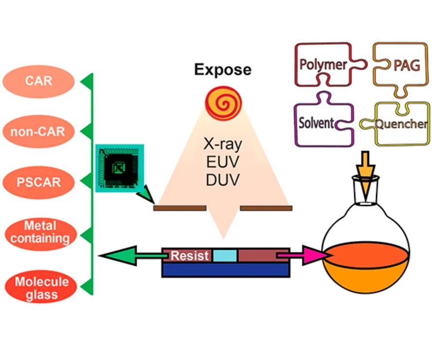
Of all these stages, lithography, in particular, determines the dimensions and topology of the microchip components. The higher the resolution of the lithography equipment used, the smaller the size of components that can be achieved. Lithography is a process for forming microelectronic components on a wafer using photoresists, that is, coatings that are sensitive to high-energy radiation (UV radiation, electrons, ions, and X-rays) and can reproduce the specified relative positions and configurations of components. A typical sequence of operations in the lithography process is shown inFig. 1. The type of lithography depends on the radiation source used in the exposure equipment (Table 1).[1][2]
![[{"id":"pYSJWKVgHG","type":"paragraph","data":{"text":"Formation of a lithographic image"}}]](/storage/images/resized/2jFQ1N9ev6ynrErTSfBTkumtYzxzhMYDVdAtysa4_xl.webp)
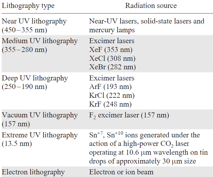
Most of modern microchips are manufactured using lithography with a 193 nm radiation source.
Resolution enhancement techniques (RETs), which include off-axis illumination of the photomask,[3] immersion,[4] phase-shift masks,[5] and multiple exposure,[6] made it possible to achieve a limiting resolution of 8 nm in ultraviolet lithography. However, the use of these techniques increases the cost of lithography, while reducing productivity, as the application of RETs increases the number of operations on the wafer. An alternative way to increase the resolution is to switch to equipment with a radiation source emitting at shorter wavelengths. Studies of lithography at a wavelength of 13.5 nm were started in the 1980s in various countries.[7-11] Currently, only the Dutch company ASML (Advanced Semiconductor Materials Lithography) possesses a technology for manufacturing lithography equipment operating at 13.5 nm wavelength; hence, this company actually holds a monopoly in the microelectronics market.
The ASML concept for the development of extreme ultraviolet (EUV) lithography is based on achieving a performance of the lithographic process comparable to that of deep ultraviolet (DUV) lithography, but offering superior spatial resolution and smaller number of operations on a substrate as a result of less RETs.[12]
However, this concept suffers from considerable drawbacks. The radiation source used in the facility developed by ASML emits highly charged tin ions produced on exposure of tin droplets of approximately 30 mm in size to a high-power CO2 laser with a wavelength of 10.6 mm. The use of this source results in the huge size of the facility (the laser system alone can take up an entire floor), a power output exceeding the megawatt level, and a consumption of almost 1 kg of tin per day, which must then be removed. The main problem with using tin is that its vapour contaminates optical filters, reflecting mirrors, and collector lenses, which puts them out of operation.[13] Even when measures are taken to protect the optics, the expensive collector needs to be reinstalled every two weeks.[14] All this results in an extremely high cost of EUV lithography equipment. The price of a single lithography machine of the NХE:3400С series may exceed 300 million euros.[1] At this price, only industrial giants such as TSMC (Taiwan Semiconductor Manufacturing Company), Samsung, and Intel can afford this equipment. This rules out the very possibility for smaller companies to compete with them on the global microelectronics market.
The need for import substitution and the development of domestic microelectronic chips has led to an increase in the scientific interest in the production of equipment and materials for lithographic processes in Russia. According to the Roadmap for the Development of X-ray Lithography in Russia developed at the Institute for Physics of Microstructures, Russian Academy of Sciences,[1] the concept being developed for X-ray lithography will reduce the cost of lithography equipment, while maintaining spatial resolution standards at the level achieved by ASML. The new technique is based on switching to a xenon laser-plasma source operating at 11.2 nm. The decrease in the wavelength will improve resolution, and the replacement of tin with xenon will extend the service life of the optical components of the system and reduce the cost of equipment and operation.[15-17]
However, switching to a new wavelength requires the development of new resists or optimization of the existing formulations for the new technologies. A resist is an integral part of lithography. Therefore, it is necessary not only to design new lithography equipment, but also to develop a resist that would be effective in a particular manufacturing process. The development of new materials for lithography requires a thorough consideration of what has already been proposed by modern science and industry. The design of a resist for the new wavelength may be performed in two ways. The first one is optimization of existing formulations by introducing functional components. The other one involves creation of something completely new. Both approaches require a thorough analysis of existing options and the selection of the optimal synthetic and engineering solutions. This analysis is given in the present review, which describes the avenues and trends of research dealing with the development of resists for DUV and EUV lithography over the last 20 years.
In the contemporary literature, there are quite a few reviews devoted to resists; however, they usually address differentiated subjects and focus on a single type of material. For example, there are reviews considering chemically amplified resists[18] and molecular glass-based resists,[19] as well as papers highlighting advances in the development of metal-based resists.[20] While preparing our review, we examined the above publications and other related papers. The most comprehensive review covering all currently available resists for EUV lithography was reported by Wang et al.[21] However, despite the broad scope of the review, the authors paid very little attention to the principles of resist operation and differences in their chemical composition, which does not provide an integrated picture. It was important for us to bring together in a single study not only a description of resist structure and the history of resist development, but also the principles of operation, chemical composition details, modification methods, and the relationship between these factors and key lithographic characteristics, while limiting ourselves to the DUV and EUV lithography ranges.
Thus, this review arranges our knowledge of resists as a relationship of the chemistry, operation mechanisms, and performance characteristics, which not only provides understanding of existing approaches, but also makes it possible to identify the most promising avenues for the development of new materials. This integrated approach is particularly important for designers who work on improvement of the lithographic properties of resists in the face of stringent industrial requirements.
2. Key characteristics of resists for DUV and EUV lithography
The development of an optimal process for the manufacture of resists is subject to the trade-off between the ease of synthesis of the components and final lithographic properties of the material. The key characteristics for any resist are as follows:
— resolution (R) characterizes the ability of a resist to transfer an image with specified minimum feature dimensions. The resolution of a resist is usually described by the half-pitch in nanometres. For periodic structures, such as lines and spaces, the half-pitch corresponds to the minimum distance between the centres of identical features and is equal to the linewidth (or the diameter of the contact opening);
— sensitivity (S) is the minimum exposure dose required to fully develop the resist in EUV and DUV lithography. The sensitivity is expressed in mJ cm–2;
— line edge roughness (LER) for the exposed area characterizes the accuracy of image transfer. LER and linewidth roughness (LWR) are measured in nm. The relationship between these two closely related values is shown in Fig. 2.
![[{"id":"PQQeebcCBm","type":"paragraph","data":{"text":"LER and LWR for a line-and-space pattern"}}]](/storage/images/resized/auQk96PEsZNScuZLTDUZRZBHo1HY1nsRhWYOJi1j_xl.webp)
Additional characteristics, which are still important for production processes, are the following:
— resist contrast characterizes the ability of a resist to generate sharp boundaries between exposed and unexposed areas. The higher the contrast, the sharper the lines and shapes of exposed features. As a rule, there is a trade-off between the sensitivity and contrast: in most cases, high-sensitivity resists have lower contrast. A contrast not lower than 4 is a generally accepted standard;
— etch resistance is a parameter depending on the type of resist, type of etching, and the substrate material used for resist deposition. Since the resist not only serves to transfer the circuit pattern onto the substrate but also acts as a protective layer during the subsequent etching processes, it must possess the required resistance to these processes. If reactive ion etching in gas plasma is used, this parameter is calculated separately for each type of gas mixture. Etching selectivity is a related parameter defined as the ratio of the substrate etching rate to the resist etching rate. High selectivity combined with high resist stability is critically important for the fabrication of microelectronic structures, as this enables the material to be etched precisely through the openings in the protective resist mask without compromising the integrity of the protective layer.
It is important to consider all of these parameters while developing resists. However, primary attention is paid to the first three parameters, that is, sensitivity, resolution, and line edge roughness. This is due to the strong relationship between these values, which is especially pronounced for chemically amplified resists. This relationship is vividly described by the RLS (resolution/LER/sensitivity) triangle (Fig. 3). The triangle illustrates a fundamental trade-off: any attempt to improve one parameter by changing the formulation inevitably leads to a deterioration of the other two parameters. Thus, the development of a chemically amplified resist requires a balanced consideration of all three vertices of this triangle.
![[{"id":"K0P431kxMz","type":"paragraph","data":{"text":"RLS triangle"}}]](/storage/images/resized/QgGviYE0o09HiMKb5C9JBQyKYjM6S1JtGztlX2Zd_xl.webp)
Chemically amplified resists have long formed the basis for most EUV and DUV lithography processes, with the scientific research and industrial design work being directed only towards fabrication of new materials of this class.[22] Currently, resists of this type remain the most numerous, the most structurally diverse, and the most thoroughly studied. In particular, commercial chemically amplified resists serve as the reference standards for evaluating new resist materials in terms of key parameters: resolution, sensitivity, and contrast.
By 2016, the following compromise between RLS values was established for commercial chemically amplified resists: a resolution of less than 16 nm, an LWR of less than 1.5 nm, and a sensitivity of less than 20 mJ cm–2.[23][24]
The indicated limits have never been final. The need to reduce the size of integrated circuit features while minimizing the use of RET requires a higher resolution of resists; however, for a smaller size of the pattern features, a smaller LER is required. Therefore, the targets for resist resolution and roughness have gradually become more stringent. By 2020, the target for resolution of prospective resists had decreased below 10 nm.[25] Reaching this frontier required a long way of development and upgrading involving not only the resist formulations, but also the associated exposure and metrological control techniques.
Back in 2011, Naulleau et al.[26] noted that the progress in the resolution of organic chemically amplified resists retarded and ceased at a level of 20 – 22 nm half-pitch. According to the results of simulation performed by the authors, one reason for the increase in roughness is photon shot noise, which is a problem not only for the resist but also for the radiation source. In 2014, Tarutani et al.[27] made an attempt to fabricate a new chemically amplified resist that would go far beyond the 20 nm threshold. The results were studied using EUV and electron beam lithography equipment. Although the final goal of a14 nm half-pitch was not achieved, lines with a 16 nm half-pitch were obtained by EUV lithography and a 15 nm half-pitch was achieved by electron beam lithography. In 2018, Tasdemir et al.[28] proved for the first time the applicability of chemically amplified resists for 11 nm half-pitch lithography. For this purpose, they developed a new normalized image log slope (NILS) correction method for EUV interference lithography, in order to compare the images for two different lithographic tools: EUV interference lithography tool and NXE ASML scanner. The 10 nm limit was overcome by using resists that contained metal atoms as nanoparticles, oxides, or oxo clusters, which started to be actively developed in the 2010s–2020s.[29] The current record resolution of 8 nm belongs to a hafnium-based resist (Inpria JB).[30]
The 8 nm resolution represents the absolute limit for a resist, which is not always necessary to achieve. For example, a modern memory chip contains approximately 80 layers, of which only about 25 layers are critical, that is, they have the minimum feature size.[1] The complexity of fabrication of these 25 layers determines the cost of the whole chip. The use of a high-resolution resist for the other layers of the chip is not cost effective. Therefore, resists with lower resolution are also widely used in industry, which provides cost optimization. The choice of a resist is dictated by the details of a particular manufacturing process. There are many different types of resists, as each group was developed to solve a specific problem, for example, to use an exposure source with a strictly defined wavelength, or to carry out ion etching processes in a gas plasma of a specified composition. Thus, the development of a resist is not merely a matter of achieving record-breaking parameters. The resist should be a processable and a convenient tool for particular production tasks.
The properties of a resist are determined by its chemical composition. However, there is no single optimal formulation. A resist of any chemical structure is a complex system comprising many components that influence its final properties.
Therefore, before comparing their characteristics, it is important to consider what types of resists exist for EUV and DUV lithography, how they differ from one another, and how their components affect lithographic characteristics.
3. Classification of resists for EUV and DUV lithography
The diversity of resists is high. Even within only DUV and EUV ranges, they can be classified in terms of various characteristics.
Depending on the photochemical processes that take place during exposure, resists are classified into positive and negative ones. The operation of positive resists involves decomposition of molecules or cleavage of functional groups on exposure to high-energy radiation, resulting in the formation of the maximum possible amount of soluble compounds. During exposure, this gives rise to areas that are soluble in developers (usually alkaline solutions). The operation of negative resists is based on polymerization reactions and the subsequent cross-linking of polymer chains (condensation) during exposure; this gives rise to insoluble areas, which remain on the substrate surface after development.
In terms of the chemical structure, three types of resists can be distinguished:
— organic resists, in which all components are organic compounds, represent the best studied and the most numerous class of resists;
— inorganic resists, the smallest class currently represented by negative resists based on aqueous zirconium and hafnium peroxo clusters;
— hybrid materials that combine the chemical properties of both organic and inorganic compounds such as silsesquioxanes or organic metal oxo clusters, in which an inorganic core is surrounded by an organic periphery.
The class of organic resists is most difficult for systematization in terms of chemical composition, as it has numerous classification criteria. Our attempt to perform a systematization reflecting the main groups of DUV and EUV resists is presented in Table 2.
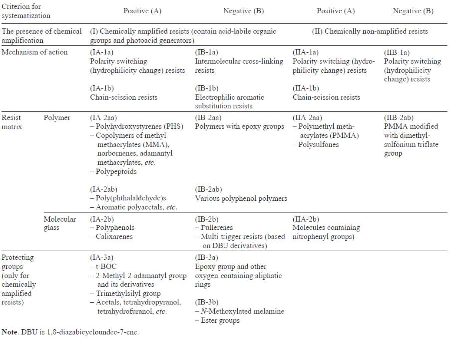
Although the proposed classification covers most of the existing organic resists used in EUV and DUV lithography, it should be regarded as provisional, as mixed systems are widely used in practice. Resists may contain polymers comprising, for example, both styrene and acrylate moieties (with a combination of various protecting groups). In some cases, a single system may even combine different image formation mechanisms.
Hybrid organic-inorganic materials can also be subdivided into groups according to several criteria. In terms of the composition, they can be classified into:
(1) silicon-containing materials, most often, hydrogen silsesquioxane (HSQ) and its organic derivatives;
(2) metal-containing compounds, which can, in turn, be classified according to the type of bond between the metal and the organic environment, into the following groups:
— metal and metal-oxide nanoparticles with an organic matrix;
— metal oxo clusters with organic ligands;
— molecular organometallic complexes.
In addition, metal-based resists can be classified in terms of the nature of the metal they contain: Hf, Zr, Zn, Ti, Sn, Al, Sb, Co, etc. It is noteworthy that the hybrid organometallic and silsesquioxane resists are negative resists in the vast majority of cases.
Each of the above types of organic, hybrid, and inorganic resists has its own benefits, drawbacks, and engineering limitations related to their chemical structure. Consideration of the principles of operation of resists, their components, and lithographic characteristics should be started with organic resists.
4. Organic chemically-amplified resists
The vast majority of positive and negative resists used in modern lithography are based on the chemical amplification principle (chemically amplified resists, CAR). The chemical amplification concept was proposed by Ito and Willson, quite long ago, in 1982.[18] Any chemically amplified resist (both negative and positive) typically contains four major components, each making a considerable contribution to the resist operation and lithographic characteristics:
(1) a chemically amplified resist is, most often, based on a polymer, the key feature of which is the presence of acid-labile protecting groups. The natures of the polymer chain and the protecting groups determine the mechanical strength, thermal stability, and the mechanism of solubility change after exposure and baking. A polymer is not the only possible type of resist matrix. It is also possible to use molecular glasses: multifunctional small-molecule compounds, such as fullerenes or calixarenes. In this case, the key parameters of the material are also determined by the nature of the compound used as the matrix;
(2) radiation-sensitive component, which generates a definite amount of free reactive species. These reactive species can be either ions or radicals. However, most often, photoacid generators are used in resist formulations. Photoacid generator (PAG) is a compound that decomposes on exposure to UV light to give a Brønsted or Lewis acid.[31][32] These compounds provide sensitivity to ultraviolet radiation and initiate changes in the solubility of the exposed film in the developer;
(3) base quencher the role of which is to selectively capture acid molecules. The presence of a quencher makes it possible to control and limit acid diffusion into unexposed areas of the film and prevent undesired reactions outside the exposed area;
(4) solvent as a medium for homogeneous distribution of the resist components, ensuring the required rheological properties for the formation of a high-quality, uniform film upon centrifugation followed by baking.
Chemical reactions in the resist occur in two stages:
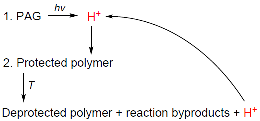
(1) during exposure of the resist, PAG releases a photoacid;
(2) the released acid diffuses into the resist mask, mainly within the exposed area, and initiates chemical reactions of polymer deprotection, polymer chain scission, or intermolecular cross-linking. This causes switching of the polarity of the resist film in the exposed areas.
Thus, the operating mechanism of a chemically amplified resist can be conceived as shown in Scheme 1 in relation to polarity switching. The key condition for the occurrence of the second-stage reactions is post-exposure bake. To ensure that the released acid performs deprotection only within the exposed area, a base quencher is added. This provides an increase in the chemical gradient of the deprotection reaction between exposed and unexposed areas.
The chemical composition of a resist determines the image formation mechanism. However, the same functional components can be used in formulations operating by fundamentally different mechanisms. These components include PAGs and base quenchers.
4.1. Photoacid generators
The choice of PAG depends on the radiation nature, the resist matrix nature, and economic feasibility. A photoacid generator should provide a high quantum efficiency of acid formation, have good solubility in the solvent used for resist formulation and good miscibility with other resist components, and possess thermal and hydrolytic stability. The strength of the acid and the size of the acid anion are the crucial factors for the selection of PAG. Currently, preference is given to PAGs that generate acids with relatively bulky anions such as trifluoromethanesulfonic acid or perfluorobutanesulfonic acid. This is due to the direct relationship between the size of the acid molecule and the diffusion coefficient of the acid in the resist film, which in turn directly influences the final resolution. The smaller the acid residue, the greater the distance by which a photogenerated proton can diffuse during the post-exposure bake. Excessive diffusion of the acid leads to an undesirable deprotection in unexposed areas, which adversely affects the resolution and LER.
Thus, for the development of chemically amplified resists, it is necessary, on the one hand, to provide the maximum quantum yield and the strength of the generated acid and, on the other hand, to ensure a strict control of acid diffusion during the post-exposure bake. The PAG efficiency is characterized by not only the quantum yield of the H+ cation. In some cases, the Dill C parameter is used for this purpose. The Dill C value quantitatively describes the rate of variation of the photoresist absorbance during the exposure, that is, the rate at which the light-sensitive component (PAG) is consumed during the exposure. This value directly affects the material sensitivity and contrast. The higher the Dill C value, the faster the photochemical reactions in the resist and the higher the resist sensitivity. The Dill C value is measured in cm2 mJ–1. Both characteristics are important operating parameters that should be taken into account for the development of resist formulations.
All PAGs used in modern resist formulations can be subdivided into ionic and non-ionic ones.
The main representatives of ionic PAGs used in positive and negative resists for DUV and EUV lithography are onium salts, namely, diaryliodonium (e.g., 1) and triarylsulfonium (e.g., 2) salts containing BF4–, SbF6–, AsF6–, PF6–, and RSO3– anions. On exposure to UV light, these salts generate Brønsted acids.[31] Triphenylsulfonium and diphenyliodonium salts are most commonly found in chemically amplified resists that operate via the polarity switching mechanism and in some negative resists containing epoxy cross-linking agents.
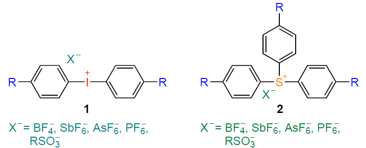
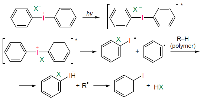
Diaryliodonium salts are relatively thermally stable and have an absorption maximum around 250 nm. This value depends only slightly on the nature of the anion or the substituent R at the periphery of the benzene ring. The quantum yield of photolysis of the diaryliodonium compounds is relatively high (approximately 0.2 in acetonitrile at a wavelength of 313 nm) and varies slightly depending on the peripheral substituents and anions.[31] A possible mechanism of decomposition of diaryliodonium salts on exposure to UV light is shown in Scheme 2.
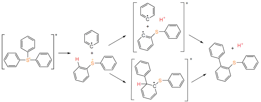
Triarylsulfonium salts are highly effective PAGs with high thermal stability, which is particularly important for photoresists that are subjected to thermal drying before and after exposure during formation of the lithographic image. The photolysis of a triarylsulfonium salt is depicted in Scheme 3.[32]
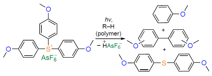
Triarylsulfonium salts have an absorption maximum in the range of 190 – 365 nm and a high quantum yield of photoacid generation; for example, in the case of compound 2 (R = OCH3 , X– = AsF6–, the quantum yield of photolysis is 0.17 at 313 nm and 0.19 at 365 nm in acetonitrile. According to a recent study by Kuznetsova et al.,[33] compound 2 (R = H, X– = C4F9SO3–) shows a quantum yield of 0.59 on exposure to radiation at 248 nm wavelength. The Dill C parameter measured for a resist formulation based on this salt is 0.022 cm2 mJ–1. The introduction of But substituents into the aryl ring of 2 (R = But, X– = C4F9SO3–) leads to an increase in Dill C to 0.03 cm2 mJ–1; however, it is accompanied by a decrease in the quantum yield to 0.30. Even the introduction of a single But group decreases the quantum yield. An increase in the Dill C value, indicating an increase in the light sensitivity, is associated with a change in the PAG optical properties: it is known that the introduction of bulky peripheral substituents can cause a red shift of the absorption peaks and an increase in the molar absorption coefficient (absorbance). In practice, while choosing between the sensitivity and the quantum yield, researchers typically sacrifice the absolute value of light sensitivity in favour of a higher quantum yield of acid generation, since this parameter has a greater effect on the pattern resolution and uniformity.
The quantum yield of PAG decomposition in the final photoresist formulation is determined by the properties of the polymer matrix. For DUV resists, it was found[34][35] that the efficiency of various PAGs varies depending on the type of polymer. For example, triphenylsulfonium salts show a higher quantum yield of acid generation and a higher Dill C when used with acrylate-based polymers. Meanwhile, diphenyliodonium salts are more efficient, although slightly, in polystyrene-based matrices (Table 3).
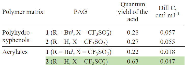
On moving to shorter wavelengths of exposure, the quantum yield of the acid, as well as light sensitivity characteristics, decrease. Resists based on an acrylate polymer matrix and exposed to 193 nm light in the presence of triphenylsulfonium salt 2 (R = H, X– = CF3SO3–) showed a quantum yield of 0.11 for Dill C = 0.029 см2 mJ–1. In the case of iodonium salt 1 (R = But, X– = CF3SOO3–), these values proved to be even lower: 0.05 and 0.012 cm2 mJ–1, respectively.[34]
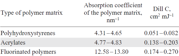
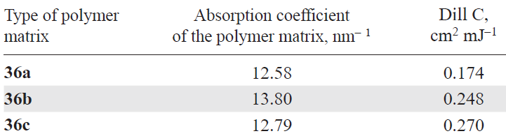
Fedynyshyn et al.[36] measured the efficiency of acid generation on exposure to EUV light in various polymer systems of chemically amplified resists, the operation of which is based on the polarity switching mechanism. The efficiency of acid generation was evaluated from the obtained values of Dill C. The authors found that the polymer matrix has a substantial effect on the acid generation efficiency of the PAG used, that is, di(tert-butylphenyl)iodonium nonaflate 1 (R = But, X– = C4F9SO3–). There is a linear relationship between the absorption coefficient of the resist polymer matrix and the efficiency of acid generation. Some results of this study are presented in Table 4. The lowest absorbance and, hence, a low Dill C value were found for polystyrene-based resists. Methacrylate-based resists demonstrated high values for both the absorption coefficient and Dill C. In addition, high characteristics were found for resists based on fluoromethacrylates and fluoronorbornenes (considered in Section 4.3.2). Thus, photosensitization of the polymer by introduction of photoactive substituents can markedly improve the properties of the whole resist by increasing the quantum yield of the acid. This opens up the possibility of targeted modification of existing polymer matrices to adjust them for new exposure sources and industrial processes.
Evaluation of the influence of the nature of various PAGs on the behaviour of a resist film carried out in relation to methyl methacrylate, methacrylic acid, and ethoxymethyl methacrylate terpolymers[37] showed that triarylsulfonium salts activate the dissolution of resist polymer films in alkaline solutions, whereas aryliodonium salts inhibit the dissolution. The highest contrast in the positive image on exposure at 248 nm wavelength, amounting to 5.8, was achieved using the terpolymer and iodonium salt 1 (R = But, X– = C6H5CH3SO3–) as PAG.
The effect of the nature of substituents present in PAGs on the lithographic properties of resists is observed only for UV and DUV ranges. In the development of resists for EUV and X-ray lithography, the increase in the absorption coefficient and the red or blue shift of the absorption maxima are no longer as critical as for materials operating in the near-UV and DUV ranges, because the mechanism of interaction of PAGs with radiation is fundamentally different in this case. It can be briefly described by Scheme 4.[38] In addition, a recent study using EUV photoemission spectroscopy to monitor in situ chemical changes taking place during the resist exposure[39] showed that the acid anion may also undergo chemical transformations during the exposure. Previously, it was believed according to the classical model that the anion remained chemically inert, serving only as a counter-ion. Thus, ionization and the subsequent transformations of both PAG components (the proton-generating cation and the anion) contribute to the overall mechanism of the photoresist operation.
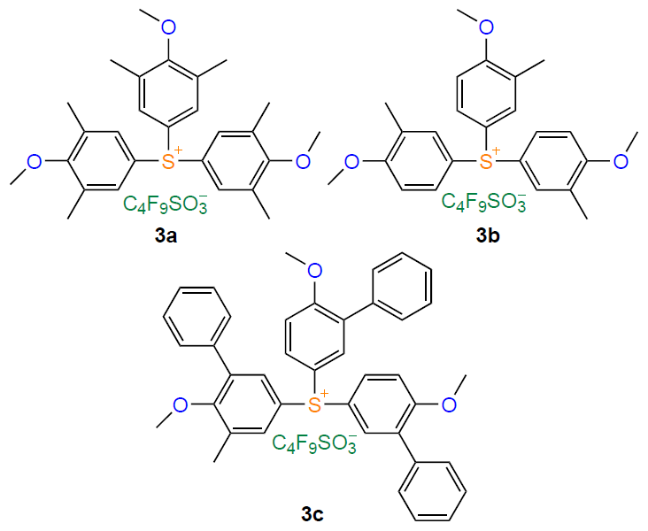
According to Asakura et al.,[40] modification of the optical properties of triphenylsulfonium salts by introducing substituents does not substantially affect the final sensitivity of the resist formulation to EUV radiation. The authors studied symmetrically substituted triphenylsulfonium salts 2 (R = H, X– = C4F9SO3–) and 3a – c. The sensitivity of the resists to EUV exposure for all samples prepared using these four acid-generating salts in combination with two different polymer matrices (polyphenol and acrylate) falls within a narrow range of 9.3 to 12 mJ cm–2.
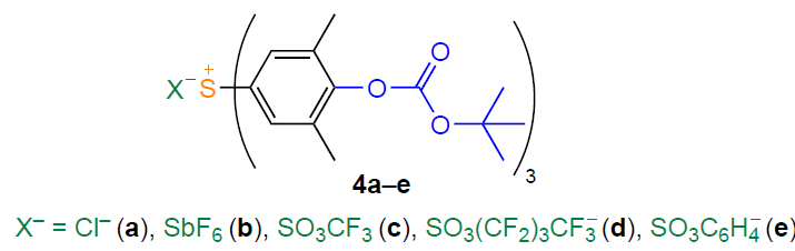
The nature of the counter-ion in triphenylsulfonium salts determines the strength of the generated acid, which is crucial for the formation of the lithographic pattern. Lawson et al.[41] investigated molecular resists based on triphenylsulfonium salt 4 with But protecting groups. They prepared five compounds differing in the X– acid anions: Cl– (4a), SbF6– (4b), SO3CF3– (4c), SO3(CF2)3CF3– (4d), and SO3C6H4– (4e). The choice of anion had a considerable effect on the key physicochemical and lithographic characteristics of the resists: solubility, film formation quality during centrifugation, sensitivity, contrast, and LER. The best results for EUV lithography were obtained for the SbF6–-containing photoacid-generating salt. A 50 nm half-pitch was achieved for line-and-space patterns with LER of 5.2 nm. The resist sensitivity was 60 mJ cm–2, which is a modest result for modern industrial processes.
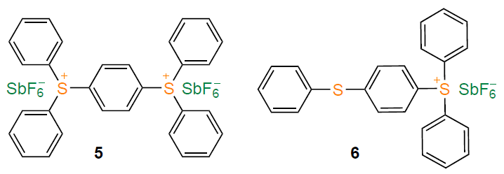
An effective method for increasing both the quantum yield and the overall light sensitivity of triphenylsulfonium salts is to increase the number of chromophore sulfonium groups in the molecule. Examples are compounds such us structures 5 and 6. Two sulfonium groups provide the most efficient photoacid generation. Furthermore, it is permissible to use a mixture of a few photoacids with different structures but the same acid counter-ion in resists. As an example, consider a commercially available triphenylsulfonium salt mixture, Cyracure ® UVI 6974, which comprises compounds 5 and 6 in 9 : 1.34 ratio.
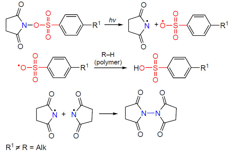
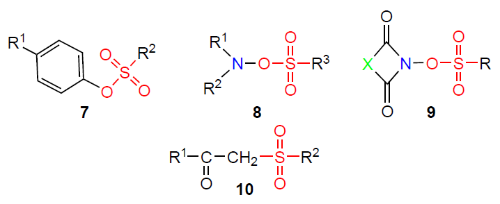
The non-ionic PAGs used in resist formulations for DUV and EUV lithography include aryl sulfonate derivatives 7, iminosulfonates 8, imidosulfonates 9, and sulfones 10. The acid generation during exposure is due to the photochemical homolytic cleavage of the C – O, N – O, or S – O bond in the PAG molecule. The resulting radicals then detach a hydrogen atom from a solvent molecule or the polymer matrix, thus generating a proton (H+) and completing the formation of a Brønsted acid.[32] The photodecomposition mechanism of non-ionic PAGs in relation to imido sulfonates is shown in Scheme 5.
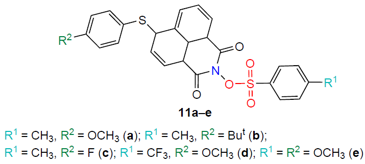
The quantum yield of acid generation by non-ionic PAGs can be adjusted by introducing substituents. Zhuang et al.[42] synthesized imidosulfonates 11a – e with various electron-donating and electron-withdrawing substituents. The highest quantum yield (0.176) was found for compound 11d (R 1 = CF3, R2 = OCH3). Electron-withdrawing substituents in the benzenesulfonic acid residue were shown to increase the quantum yield. Studies of resist compositions prepared by mixing these salts with a polypropylene glycol polymer matrix demonstrated a direct correlation between the quantum yield of the acid and the final resist sensitivity. The composition based on the most effective compound 11d (R1 = CF3, R2 = OCH3) exhibited the shortest exposure time (2 min) to 253 nm light.
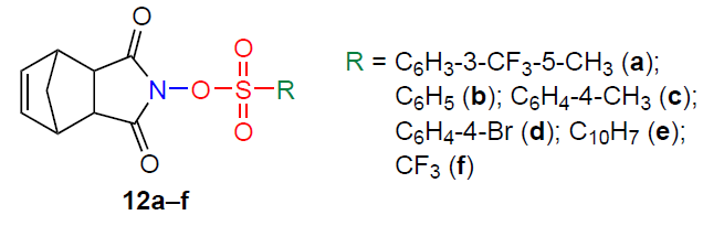
The pronounced effect of substituent at the sulfonic acid residue is also confirmed by a recent study by Zhang et al.[43] The authors synthesized and studied a series of PAGs based on norbornene imides with various substituents (12a – f). The photoacid generation quantum yields were measured in an acetonitrile solution on exposure to light at 254 nm wavelength. The best quantum yields were obtained for compounds 12e (0.328) and 12f (0.256). All of the prepared compounds had an optical absorption peak at 190 – 200 nm, which accounts for their sensitivity to DUV radiation.
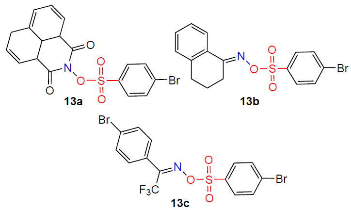
Many non-ionic sulfonate PAGs exhibit good sensitivity to DUV radiation. Deng et al.[44] reported resists based on brominated poly(phthalaldehyde) in combination with nine PAGs. It was found that resists containing aryl, iminosulfonate, and imidosulfonate PAGs are sensitive to DUV radiation. High sensitivity to EUV was inherent only in resists with imino/imidosulfonate PAGs 13a – c containing bromine. The sensitivity of resist compositions based on these compounds ranges from 10 to 15 mJ cm–2, which meets current industrial requirements.
Quite often, ionic and non-ionic PAGs are directly immobilized (covalently inserted) into the polymer matrix. This approach provides a more uniform distribution of the acid catalyst and, at the same time, limits the diffusion of the acid anion, since it is bound to the matrix. This markedly increases the resolution of resists. Particular examples of such polymers with immobilized PAGs will be discussed in the subsequent Sections.
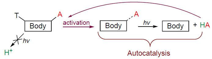
In order to increase the PAG efficiency, acid amplifiers, that is, compounds that decompose under the action of acid catalysts to give an additional amount of acid, are used in some cases in resist formulations. The process is autocatalytic when the photogenerated acid is relatively strong and catalyzes the decomposition of the acid amplifier. Most often, acid amplifiers are used in chemically amplified resists meant for EUV and DUV lithography.
To improve the image quality in a photoresist, acid amplifiers must meet the following requirements:[45]
(1) thermal stability in the absence of an acid, at least under lithographic conditions;
(2) rapid decomposition in the presence of an acid catalyst;
(3) the ability to generate strong acids.
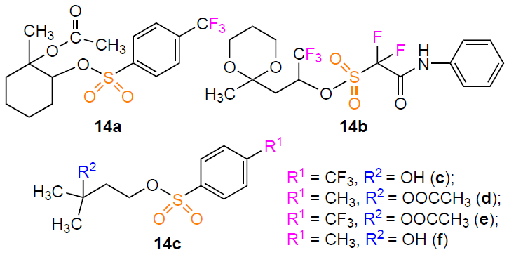
Most often, these compounds are structurally similar to non-ionic PAGs, such us arylsulfonates and sulfones, for example, compounds 14a – c. Preference is given to acid amplifiers capable of generating strong sulfonic acids, e.g., those containing fluorine.
A typical acid amplifier consists of three components (Scheme 6): the body, the acid-sensitive trigger (T), and sulfonic acid precursor (A).[46-48]
The introduction of acid amplifiers is intended to improve the lithographic performance of the resist, which is confirmed in a number of studies. On exposure to EUV light, compound 14b mixed with a resist based on the polyhydroxystyrene matrix provided a considerable enhancement of LER from 4.6 nm (control sample containing no amplifier) to 2.1 nm for a line-and-space pattern with a half-pitch of 50 nm.[46][49] The addition of compound 14a to a polystyrene-based resist improved the sensitivity and LER characteristics (16.6 mJ cm–2, LER of 4.5 nm) compared to those of the parent resist (21.7 mJ cm–2, LER of 8.2 nm) in the EUV formation of a line-and-space pattern with a 38 nm half-pitch.[50] The addition of acid amplifiers 14c – f resulted in a considerable improvement of the resist sensitivity; for compound 14c, it amounted to 1.9 mJ cm–2 (vs. 7.6 mJ cm–2 for the control sample). However, this improvement came at the cost of a corresponding deterioration of LER, which increased from 4 to 7.9 nm.[51] This result clearly demonstrates that acid amplifiers are not a panacea and do not eliminate the fundamental limitations described by the RLS triangle.
The acid amplifiers can be covalently inserted into the polymer matrix, as shown, for example, by Kruger et al.[51] Although this approach provided a decrease in LER compared to that of the control sample, lower LER values were found for systems in which the amplifier was simply physically mixed with the resist.
The introduction of acid amplifier directly into the PAG molecule was studied by Joo et al.[52] The authors synthesized PAGs containing an amplifier. However, this approach was deemed unsuccessful. The main reason was as follows: the use of bulky anionic groups to limit acid diffusion reduced the maximum permissible concentration of PAGs in the formulation. As a result, the introduction of these PAGs into the resist formulation did not lead to a considerable enhancement of key lithographic parameters.
Thus, PAG is an essential component of chemically amplified resists. Although the same processes in resists can be initiated using different PAGs, their selection must be based on the nature of the polymer matrix and protecting groups.
4.2. Base quenchers
Both photoactive and non-photoactive bases are used as base quenchers. The addition of these compounds improves the key lithographic characteristics of resists by more accurate control of the acid diffusion.
There are two types of photoactive bases: photobase generators and photodecomposable bases. These agents operate through opposite mechanisms. The photobase generators are compounds that produce either ammonia or an amine (primary, secondary, or tertiary) on exposure to light. Currently, there is a large number of known compounds that can act as photobase generators, such as o-acyloximes, urethanes, sulfonamides, formamides, α-aminoketones, aminimides, nifedipines, and some other compounds.[31][53] Similarly to PAGs, photobase generators can catalyze the key processes of image formation on exposure to light. However, base catalysis has not found wide use in resist technology. These compounds are also rarely used as base quenchers. Their limited use is mainly due to specific chemical properties of many photobase generators. During the photoreaction they often form volatile compounds that can adversely influence the quality of the lithographic image and cause contamination of the optical parts of the equipment.
Nevertheless, successful examples of the use of photobase generators have also been reported. For example, Wang et al.[54] showed that the addition of a trisubstituted amine improved the general quality of the image (decreased the mask defect level) and increased the exposure latitude, that is, the exposure dose range in which the resist can form images of acceptable quality; no pronounced changes in LWR took place.
In turn, a photodecomposable base is a base that decomposes upon exposure into neutral molecules without affecting acid generation. In unexposed areas, a photodecomposable base remains reactive areas.[55-57] Triarylsulfonium or diaryliodonium salts with either a hydroxide (OH–) or a carboxylate anion are used, most often, as photodecomposable quenchers in resist formulations.[55][56] The use of photoactive quenchers is more effective: unlike common bases such as tributylamine, which are transparent to DUV and EUV light, photodecomposable bases serve as an additional photosensitive component that increases the sensitivity of the whole resist composition. In addition, it was shown that in the case of long-term exposure (high doses), the addition of such bases prevents the collapse of the exposed pattern.[56] The stability to collapse directly depends on the concentration of the photodecomposable base in the composition. This was demonstrated in an experiment using a resist based on a methyl methacrylate matrix. After the addition of 40 mol.% triphenylsulfonium hydroxide (relative to the molar amount of triphenylsulfonium nonaflate used as PAG) and irradiation with an ArF laser (193 nm), no pattern collapse takes place even when the dose is 28 mJ cm–2 and the exposure time is 60 min. Another benefit is that acid capture occurs only in unexposed areas, which increases the acid yield.
The structure of a non-photoactive base quencher, in turn, has a considerable effect on the efficiency of acid catalysis. This is clearly exemplified by a resist based on a polystyrene acrylate matrix with triphenylsulfonium triflate as PAG.[58] The addition of quencher 15a resulted in a higher Dill C parameter (7.37 × 10⁻⁴ cm2 mJ–1) than the introduction of quencher 15b (6.36 × 10⁻⁴ cm2 mJ–1) for X-ray lithography.
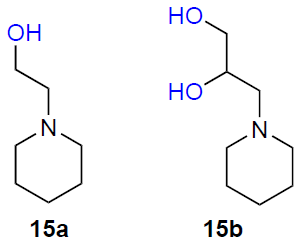
Even micromolar amounts of a quencher per gram of the composition can considerably change the observed efficiency of the process. One possible explanation for this effect is associated with the number of polar functional groups of the quencher that form hydrogen bonds with the generated acid: the more such groups in the quencher, the higher the amount of the acid that the quencher can bind, which accounts for the observed differences in the resist characteristics.
The concentrations of photodecomposable quenchers and PAGs are the primary variables used to manage the trade-offs within the RLS triangle. Kozawa[59] carried out a theoretical study to determine the optimal concentrations of components and the expected sensitivity to form 11 nm half-pitch structures at different roughness levels. When LWR was 10%, the optimal total concentration of the photosensitizer (PAG + photodecomposable quencher) was ~ 0.4 nm−3, with the predicted sensitivity being 50 mJ cm−2. In the case of LWR of 20%, these values were 0.20 – 0.22 nm−3 and 30 – 40 mJ cm−2, respectively.
Manouras et al.[60][61] selected the optimal ratio of triphenylsulfonium triflate (PAG) and aminoanthracene (base quencher) for chemically amplified chain scission resists for EUV lithography. The authors tested resist formulations containing 4 – 7 mass % PAG relative to the polymer mass and 5, 10, and 15 mass % aminoanthracene relative to the PAG mass. It was found that the higher the concentration of the base quencher, the greater the exposure dose (energy) required to form an image. In some cases, excess quencher can lead to a considerable deterioration of LER: roughness was always lower when the quencher concentration was 5% than when it was 10%. However, the best results were achieved for the highest concentrations used: 7% PAG and 15% base quencher, which is an exception to the trend derived by the authors. A line-and-space pattern with half-pitch of 25 and 22 nm and LER of less than 3 nm was obtained. The exposure dose was ~ 18 mJ cm–2.
As a rule, modern commercial resists contain 10 – 30 mass % base quencher relative to the mass of PAG.
4.3. Chemically amplified polarity switching positive resists
The matrix and its functional groups determine the main properties of the resist, in particular they determine the mechanism of formation of the lithographic image. The resists with a mechanism of action based on a catalytic change in the hydrophilicity of polymer side groups (polarity switching) are traditional materials for lithography with 248- and 193-nm light sources. The polymer matrices used for these resists are polystyrene and acrylates.
4.3.1. Polystyrene-based resists
The first resist based on the principle of acid-catalyzed deprotection was an IBM resist containing tert-butoxycarbonyl (t-BOC) protecting groups. This resist represented a two-component system consisting of poly(4-tert-butoxycarbonyloxystyrene) and PAG.[18]
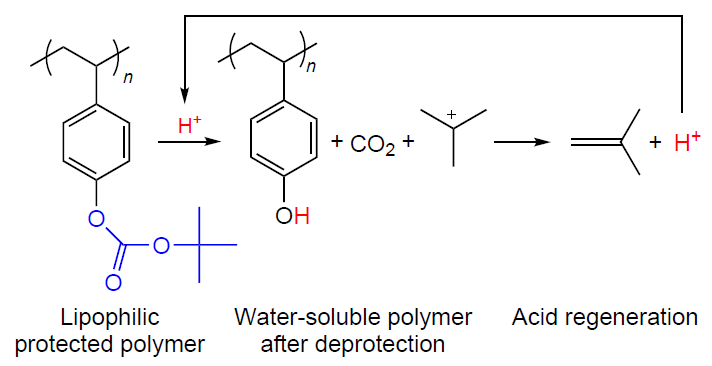
The phenolic groups of poly(4-hydroxystyrene) (PHS) were protected by acid-sensitive t-BOC group. This protecting group is thermally stable up to 190°C in the absence of acids. In the presence of an acid released upon exposure, this lipophilic polymer is converted, on heating to 100°C, into an unprotected polymer containing phenolic groups and releases carbon dioxide, isobutylene, and a proton. The deprotection reaction is a catalytic acidolysis that does not require a stoichiometric amount of water; thus, the photochemically generated acid is not consumed in a single reaction, but is regenerated for numerous transformations. The acid-catalyzed deprotection converts a lipophilic polymer into a hydrophilic one, thus providing a substantial change in the polymer polarity and, hence, in the solubility (Scheme 7). However, these resists have significant drawbacks: highly lipophilic films are prone to cracking during development in aqueous solutions, have poor adhesion to the substrate, and exhibit excessive shrinkage in exposed areas during post-exposure bake due to the release of carbon dioxide and isobutylene.[62] In addition, after deprotection, these polymers are dissolved in water much faster than similar formulations based on phenolic novolac resins and naphthoquinone diazide, which makes them poorly compatible with standard developers such as tetramethylammonium hydroxide (Me4N)+OH–.[18]
Currently, resists based on PHS alone are rarely used for EUV and DUV lithography; most often, mixed systems involving methacrylate are employed. These polymers are obtained using the following approaches:
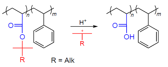
— copolymerization with various monomers, most commonly, methacrylates. In this case, the protecting groups are located at the methacrylic moiety, which markedly changes the properties of the resist films compared to the properties of resists based only on styrene. A considerable distinction is that the conversion of an ester to a carboxylic acid (Scheme 8) leads to a greater change in the polarity and solubility than the conversion of phenyl carbonate to phenol. This makes it possible to generate images at a lower degree of deprotection. The solubility of t-BOC-protected PHS polymers in alkaline aqueous solutions is achieved by removing more than 90% of the groups. The polymer solubility is effectively reduced when only 10% of units contain protecting groups.[18]
— Combinations of various protecting groups (e.g., t-BOC and the glycidyl methacrylate group).[63]
— Incorporation of PAG molecules and other photoactive components directly into the polymer chain (immobilization of PAGs and quenchers).
Copolymers (16) of 4-hydroxystyrene (4-HS), styrene (St), and methacrylates (MA) are used most often in commercial compositions. The corresponding resists are known as ESCAP (environmentally stable chemical amplification positive) type resists.
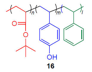
The polymer matrix of ESCAP resist is a terpolymer obtained by terpolymerization of the following monomers:
— 4-hydroxystyrene (provides the base for the matrix and the polarity),
— styrene (improves thermal stability and mechanical strength),
— tert-butyl acrylate (introduces acid-labile protecting groups, which play a key role in the image formation).
The ratio of monomer units depends on the resist brand and the target properties. For example, Brainard et al.[51] used the 4-HS/St/t-BOC-MA ratio of 65/15/20 mass %. This polymer in a resist containing bis(4-tert-butylphenyl)iodonium perfluorobutanesulfonate as a PAG and (Bu4nN)+OH– as a quencher showed a sensitivity of 7 mJ cm–2 and a moderate LER of 4 nm for 60 nm line-and-space patterns. Singh et al.[39] used a model system consisting of 4-HS/St/t-BOC-MA in 39.5/17.5/42.9 mass % ratio. As PAG, the authors used 4-(methylphenyl)diphenylsulfonium nonaflate, while trioctylamine was the quencher. The authors concluded that the protecting group is eliminated not only during catalytic deprotection, but also during exposure to EUV radiation.
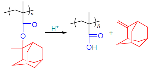
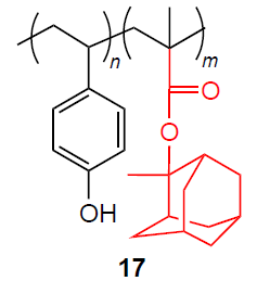
Apart from the t-BOC group, other protecting groups can also be used. A common protecting group in modern resist formulations is the 2-methyl-2-adamantyl group. This group is introduced by copolymerization of 4-hydroxystyrene with 2-methyl-2-adamantyl methacrylate 17. In the presence of acids, the 2-methyl-2-adamantyl group can be removed in the same way as t-BOC. This is due to the ability of the adamantyl group to form an exocyclic double bond, which facilitates its elimination upon protonation (Scheme 9). According to some studies, adamantyl groups are more effective than t-BOC.[64] A study of PHS-based polymer matrices with t-BOC protecting groups in one case and 2-ethyl-2-adamantyl groups in the other case revealed the influence of the nature of the protecting group on the efficiency of acid formation on exposure to an electron beam with an energy of 75 kV (ELIONIX, ELS-7700). An increase in the content of t-BOC groups to 35% reduced the efficiency of acid formation from 0.12 (0% protecting groups) to 0.1 (35% protecting groups), whereas a similar increase in the content of 2-ethyl-2-adamantyl groups increased the efficiency from 0.12 (0% protection) to 0.16 (35% protection).
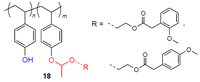
Other possible protecting groups are trimethylsilyl groups and acetal groups including 1-ethoxy-1-ethoxy-, 1-methoxy-1-ethoxy-, 1-methoxy-1-methylethoxy-, 1-butoxy-1-ethoxy-, and 1-benzyloxy-1-methylethoxy groups.[65] However, currently, preference is given to cyclic tetrahydropyranyl and tetrahydrofuranyl groups. The introduction of bulky acetal groups increases the stability of resists to reactive-ion and plasma etching. Fujimori et al.[66] synthesized PHS polymer matrices with bulky acetal groups (18). Resists manufactured using these matrices demonstrated an integrated improvement of performance:
— etch resistance increased by 40% compared to that of resists based on matrices containing the 1-methyl-1-ethoxyacetal groups;
— in a 150 nm half-pitch line-and-space pattern, LER decreased from 6.6 nm (for the matrix containing 1-methyl-1-ethoxyacetal protecting groups) to 4.4 nm.
The subsequent works using these materials showed that the introduction of bulky acetal groups also decreases the gas evolution in resist films during exposure. Using chemical modification of the polymer and PAGs (the introduction of bulky groups at the periphery of the triphenylsulfonium benzene rings), Masuda et al.[67] were able to decrease the total amount of released volatile compounds from approximately 400 × 1011 molecules per cm–2 to a level below 20 × 1011 molecules per cm–2. The resist exhibited good sensitivity to EUV radiation (12 mJ cm–2) and a resolution of 32.5 nm. It was found that molecular (unbound) PAGs are the major contributor to the amount of volatile substances released from PHS-based resists. Kobayashi et al.[68] investigated the outgassing of t-BOC-protected polystyrene polymers, depending on their chemical composition. The authors used polymers with various ratios of protecting groups and various contents of PAG and base quencher. The gases released from the resist film were detected by two methods: measurement of pressure change upon outgassing and gas chromatography — mass spectrometry (GC/MS). In both cases, the lowest amount (1014 molecules cm–2 according to GC/MS) of gaseous products was found for the sample in which no PAG was used.
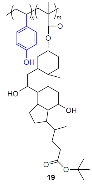
Ji et al.[69] reported a laboratory resist sample for DUV lithography based on a polymer matrix prepared by copolymerization of 4-(hydroxystyrene) with t-BOC-protected cholic acid methacrylate 19. The samples with the monomer ratio n = 50; m = 50 exhibited the following characteristics:
— high thermal stability up to 213°C (glass transition temperature); an increase in the fraction of cholic acid moieties resulted in a decrease in thermal stability;
— high sensitivity (7.5 mJ cm–2) to radiation with a 248 nm wavelength; the resist also had a rather large film thickness (approximately 340 nm);
— the ability to form a lithographic image: a line-and-space pattern with a half-pitch of 250 nm was used as a test.
Immobilization of photosensitive agents within the polymer chain is a way to improve the lithographic performance. An early example of the introduction of PAGs into a PHS polymer is the synthesis of PHS polymers containing sulfonic units (20a).[18] It was established that these polymers possess intrinsic photoactivity (they generate acid on exposure to radiation), but they have low sensitivity to DUV radiation.
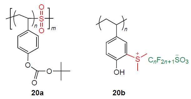
An additional introduction of a molecular PAG was required to increase the efficiency in the DUV range. Tarascon et al.[70] investigated polystyrene polymers with sulfonic units by adding three various PAGs: triphenylsulfonium trifluoromethanesulfonate, triphenylsulfonium hexafluoroarsenate, and 2,6-dinitrobenzoyl tosylate. It was found that the properties of the resist film depend, to a large extent, on the PAG added to the resist formulation:
— triphenylsulfonium trifluoromethanesulfonate increased the resist sensitivity when added in amount of 5% of the polymer mass; the result was 4 mJ cm–2 for a contrast of 4.7;
— tosylate derivatives substantially increased the contrast to 18 – 22 and sensitivity to 26 mJ cm–2 for a PAG content of 15% of the polymer mass. As the tosylate amount decreased, these characteristics deteriorated.
Another example of PAG integration into a PHS polymer chain is resists 20b developed by Liu and Wang,[71] who covalently attached a photosensitive agent to the periphery of the polystyrene benzene rings. As PAG, the authors used triphenylsulfonium salts. The purpose of this work was to develop a polymeric photoactive matrix with a high solubility in standard process solvents, since most low-molecular-weight triphenylsulfonium salts, including the studied ones, have poor solubility. The integration of perfluoroalkylsulfonate (n = 1, 4) salts into the polar matrix resulted in a material that was readily soluble in ethylene glycol monoethyl ether and ethyl lactate (≥10 mass %), partly soluble in cyclohexanone (10 mass %) and butanone (1 mass %). To endow the material with a solubility in propylene glycol monomethyl ether acetate (PGMEA), it was necessary to esterify most of the hydroxyl groups of the polystyrene with the t-BOC protecting groups. The resulting material showed a sensitivity that complied with industry standards (24 mJ cm–2) on exposure to a KrF laser. However, the preliminary pattern with a 180 nm line width cannot be used to evaluate the resolution and LER limits of this resist.
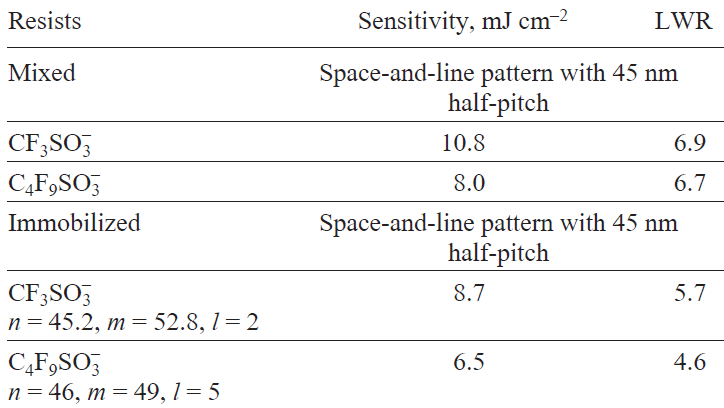
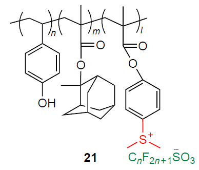
A more popular way of integration of triphenylsulfonium salts into PHS polymers is the copolymerization of 4-hydroxystyrene with monomers containing sulfonium salts. Thiyagarajan et al.[72] investigated resists with a polymer matrix based on 4-hydroxystyrene and 2-ethyl-2-adamantyl methacrylate terpolymer incorporating a covalently bound photosensitive moiety, namely, phenyl methacrylate 4-dimethylsulfonium triflate (n = 1) or nonaflate (n = 4) (21). Exposure to EUV radiation showed that these resists exhibited better lithographic characteristics than their analogues obtained by physical mixing of a 4-hydroxystyrene-2-ethyl-2-adamantyl methacrylate copolymer matrix with molecular PAG: (4-methylphenyl)dimethylsulfonium triflate or nonaflate (Table 5). An increase in the fluorine content of the PAG counter-ion in both mixed and immobilized forms has a beneficial effect on the sensitivity of the resists.
On exposure to EUV radiation, polymers based on t-BOC-protected poly(4-hydroxystyrene) with immobilized sulfate onium salts reported by Tarutani et al.[73] exhibited the highest resolution of 24 nm half-pitch for a sensitivity of 14.1 mJ cm–2 and LWR of 5.3. A resist based on a mixed polymer matrix and a molecular PAG achieved a resolution of only 26 nm half-pitch with a lower sensitivity (16 mJ cm–2) and greater LWR (6.0). In a later study by Tarutani et al.,[74] the lithographic performance of these resists was improved. An increase in the hydrophobicity of the polymer matrix by increasing the content of protecting groups improved the resolution to a half-pitch of 16 nm; however, this gain in resolution came at the cost of sensitivity, which deteriorated to 24 mJ cm–2. A subsequent study[75] addressing the dependence of sensitivity on the resolution showed that the stable formation of structures with a half-pitch of 15 nm requires a resist sensitivity of less than 30 mJ cm–2. This requirement stems from the need to minimize the effect of photon shot noise on the image quality.
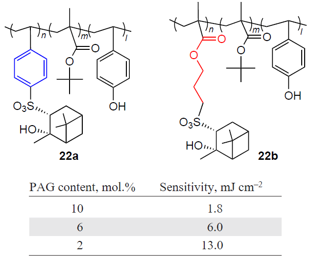
Arimitsu et al.[76] prepared and investigated polymers with immobilized PAGs 22a,b. The deprotection was faster for resists 22b than for resists 22a and, as a consequence, resists 22b had a higher sensitivity on exposure to light at 254 nm wavelength. The authors attributed this result to the presence of long, flexible bridges to the sulfonic acid groups, which facilitated more efficient acid diffusion. The number of immobilized PAG units in the copolymer affected the photosensitivity. For polymer 22b, the following dependence was established:
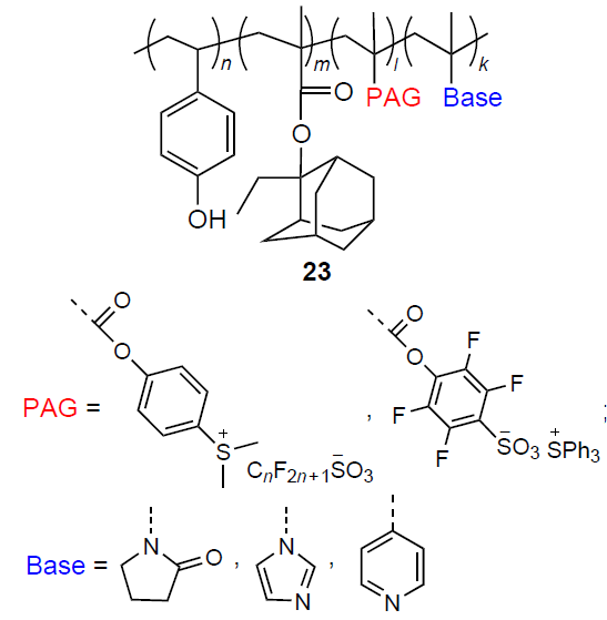
Wang et al.[77] investigated promising resists for EUV lithography; the resist polymer matrices contained both PAG and base quencher 23 in the immobilized state. The limiting resolution was estimated using electron beam lithography. The best result, that is, a 30 nm half-pitch, was achieved when phenyl methacrylate 4-(dimethylsulfonium triflate) was used as the bound PAG and a pyridine moiety was the base quencher. Unfortunately, the sensitivity of these resist formulations to EUV radiation was not addressed in this study.
As a rule, PHS-based resists are used as positive resists. However, Gonsalves et al.[78] studied the copolymer of 4-(hydroxystyrene) and 2-(4-methoxybutyl)-2-adamantyl methacrylate, which formed a negative image upon EUV exposure (13.4 nm, 92.5 eV). On exposure to lower doses, the material behaved as a positive resist. The resolution obtained for the negative image markedly exceeded that of the positive image.
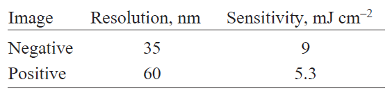
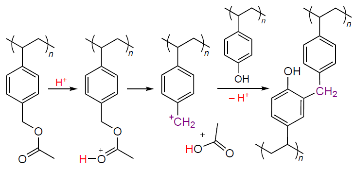
The formation of negative images at doses considerably exceeding those required for positive images is characteristic of certain groups of resists used in DUV and EUV lithography.[79][80] In these resists with a specified type of exposure, at high doses, the quantum yield of the cross-linking reaction exceeds the quantum yield of chain cleavage. As a result, when a certain energy threshold is exceeded, cross-linking processes start to predominate, leading to a decrease in the solubility of the exposed areas and the formation of a negative image.[80] This behaviour for ESCAP type resists is caused by the occurrence of the following parallel reactions:
— cationic polymerization (in this case, intermolecular cross-linking): photogenerated acid catalyzes the intermolecular cross-linking of polymer chains;
— radical polymerization (intra- and intermolecular cross-linking): high-energy radiation causes bond cleavage in the polymer backbone; the resulting radicals are involved in both intra- and intermolecular cross-linking.
Since these processes are limited by acid diffusion and the rapid loss of electron energy within the material, no effective cross-linking occurs in unexposed areas, which ultimately leads to increased resolution for the negative mask. These processes are similar to those occurring in negative resists in which the lithographic image formation is based on electrophilic substitution reactions (Scheme 10).[65][81]
4.3.2. Acrylate-based resists
Chemically amplified acrylate resists are the main types of commercial resists used for DUV lithography at a wavelength of 193 nm. The main representatives of these resists are copolymers of methyl methacrylates with 2-methyl(ethyl)-2-adamantyl methyl acrylate, norbornene, norbornene maleic anhydride, and acrylates bearing tetrahydrofuranyl and γ-butyrolactone groups. The reason for introduction of bulky substituents is directly related to the requirement for the resist to have high plasma etch resistance. This resistance correlates with the carbon content of the material: the higher the carbon content and the lower the oxygen content, the greater the resistance to plasma etching. Hence, the incorporation of large alicyclic moieties (norbornyl or adamantyl) into a polyacrylate matrix is a standard technique for improving the resistance to plasma etching.[18][82] Most resists of this type are designed for dry development processes involving plasma-chemical or ion-beam etching.[83][84]
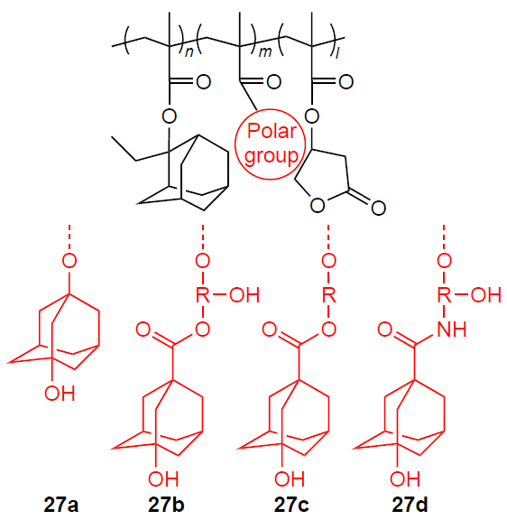
Some examples of polymers (24 – 26) used in commercial resists for immersion lithography at 193 nm wavelength can be found in the literature.[85-87] Diaryliodonium salts are added as PAGs to the IBM V2 resist; in all other indicated resists, triarylsulfonium salts are used.
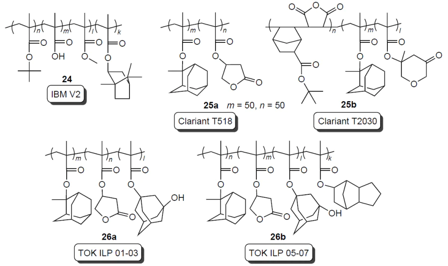
These resists are well suited for forming three-dimensional patterns with a film thickness of 100 – 150 nm and a resolution of up to 45 nm by the immersion lithography technique using a 193 nm wavelength.[85]
Table 6 presents the ranges of sensitivity and roughness for acrylate matrix-based resists 25a and 26a.[88] The authors formed patterns with 100 nm resolution using various post-exposure bake (PEB) conditions. In all formulations, triphenylsulfonium nonaflate was used as PAG, while trioctylamine served as the base quencher.
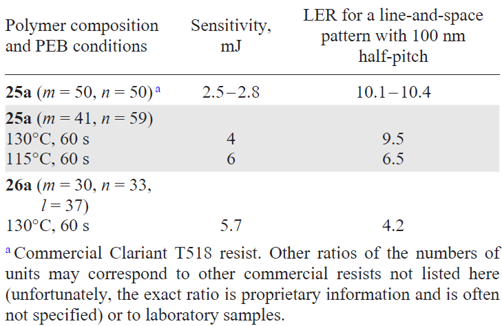
A change in the PEB conditions had a considerable effect on LER of the resist based on polymer 25a (m = 41, n = 59). The presence of polar hydroxyadamantyl groups in polymer 26a inhibited the acid diffusion within the resist film, thus leading to a decrease in LER; the lowest LER values were obtained for the resist based on this polymer. Tanagi et al.[89] synthesized terpolymers 27 of acrylates containing a 2-ethyl-2-adamantyl protecting group, a lactone protecting group, and various hydrophilic polar groups: 3-hydroxy-1-adamantyl methacrylate (27a), methacryloyloxy hydroxyalkyl 3-hydroxy-1-adamantanecarboxylate (27b), methacryloyloxyalkyl 3-hydroxy-1-adamantanecarboxylate (27c), and methacryloyloxyalkyl 3-hydroxy-1-adamantanecarboxamide (27d). The authors studied the effect of the nature of the polar group on the acid diffusion in the resist film and, hence, on the resolution and LER. All the resists demonstrated good sensitivity to EUV radiation (3.3 – 6.4 mJ cm–2). The best result of 3.3 mJ cm–2 was obtained for resists based on polymer 27c. The limiting resolution and LER of these materials were evaluated using electron beam lithography techniques. It was found that an increase in the length of the alkyl chain in the polar group and the presence of polar substituents in the chain spacers enhance the inhibitory effect on acid diffusion. The best roughness characteristics were found for resists based on polymer 27b: for line-and-space patterns of 100 nm half-pitch, LER was 7.5 nm at an exposure dose of 35 mC cm–2 and 7.2 nm for 90 nm half-pitch at a dose of 45 mC cm–2.
The nature of substituents in the polymer chain has a considerable effect on the overall mechanisms of resist operation. Kang et al.[90] investigated the deprotection kinetics in polymers 25a (m = 50, n = 50 and m = 41, n = 59), used in resists for DUV lithography at 193 nm. A simple kinetic model described the dependence of the degree of deprotection on the reaction time and photoacid concentration. According to this model, the rate constant for deprotection decreases with increasing content of lactone groups. This is attributable to decreasing mobility of the released acid as it forms hydrogen bonds with the polar groups of γ-butyrolactone. Similarly, the photoacid can form hydrogen bonds with the carboxyl groups of methacrylic acid, which also slows down the deprotection reaction. The decrease in the deprotection rate lowers the resist sensitivity, but, on the other hand, it has a beneficial effect on LER values (see Table 6).
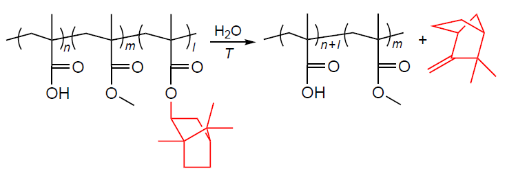
Significant results were obtained by Bulgakova et al.,[91][92] who worked on chemically amplified resists for DUV and EUV lithography based on terpolymers of methyl methacrylate, methacrylic acid, and either isobornyl acrylate or isobornyl methacrylate. The prepared polymer matrices were studied in combination with various PAGs. Exposure was performed by UV light (λ ≈ 254 nm, intensity of 0.3 mW cm–2), EUV light (13.5 nm), and an electron beam. For all types of exposure, the best lithographic properties were found for the resist based on the isobornyl acrylate copolymer. The isobornyl acrylate/methyl methacrylate/methacrylic acid composition with 53/27/20 mass ratio exposed to EUV radiation showed a sensitivity of 5 mJ cm–2 and a contrast of 9.7; this markedly surpasses these characteristics of similar commercial resists. Among PAGs, the best lithographic performance was provided by sulfonium salts, namely, triphenylsulfonium triflate and a mixture of 4-(thiophenylene)phenyldiphenylsulfonium antimonate (10 mass %) and bis(4-thiophenylenediphenyl)sulfonium antimonate (90 mass %), which generate strong acids, trifluoromethanesulfonic acid and fluoroantimonic acid, on exposure to radiation. A decrease in the electron beam energy from 30 to 10 keV and increase in the PAG concentration improved the sensitivity of chemically amplified resists. The resists containing isobornyl acrylate and isobornyl methacrylate units exhibited high plasma resistance in an Ar + SF6 plasma, with etching rate being more than an order of magnitude lower than that of silicon. It was also shown that the resist sensitivity depends on the content of isobornyl acrylate units in the polymer: as their number increases, the sensitivity of the resist decreases, which is due to incomplete hydrolysis of these units during post-exposure bake. Scheme 11 depicts the hydrolysis of the isobornylmethyl methacrylate group.
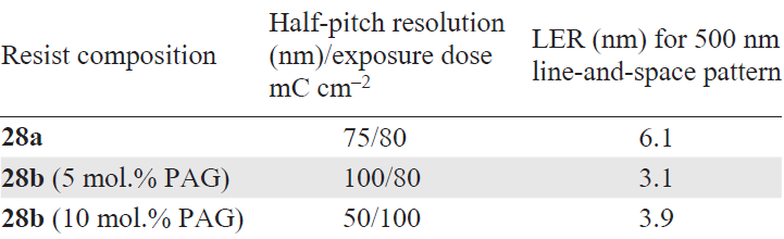
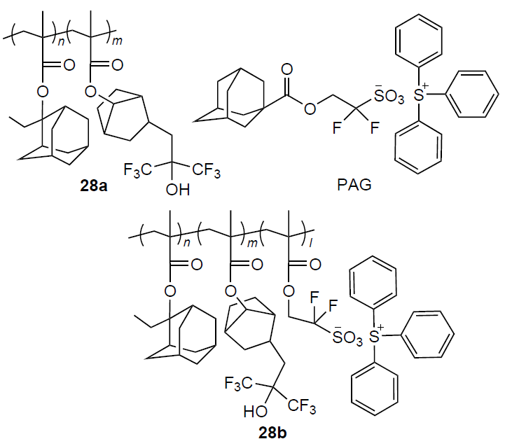
As in the case of PHS polymers, immobilization of PAG within an acrylate matrix can improve the lithographic properties of the final resist. Yamamoto et al.[93] demonstrated this fact by comparing resists with a polymer matrix containing both norbornene and adamantyl groups. In one system, PAG was added as a separate component, being mixed with polymer matrix 28a, while in the other cases, polymer 28b was synthesized with PAG being chemically bonded to the backbone. Exposure of these samples to a KrF laser (248 nm) and EUV radiation revealed differences in the properties of the resists. In the case of the polymer covalently bound to PAG, swelling upon exposure was less pronounced. Swelling of the polymer upon exposure may cause pattern deformation or collapse, which markedly limits the resolution. Therefore, the polymer behaviour during swelling directly affects the achievable resolution and the cross-sectional shape of the lithographic pattern. The resolution and LER of the obtained resists were evaluated by electron beam lithography. Table 7 presents characteristics of these resists, which attest to an increase in resolution with increasing amount of immobilized PAG. In all cases, resists based on the polymers containing covalently bound PAG had lower LER values.
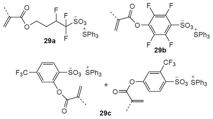
Wang et al.[94] investigated polymers with structurally diverse immobilized PAG. The authors evaluated the quantum yields (Table 8) of the acid genegation for the copolymer of 4-hydroxystyrene with 2-methyl-2-adamanthyl methacrylate (17) and the copolymer of 2-methyl-2-adamanthyl methacrylate with γ-butyrolactone acrylate (25а) containing various immobilized PAGs (29a – c). The best results were obtained using matrix 17.
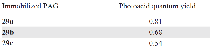
The prepared perfluoroalkyl derivative 29a possesses pronounced electron-acceptor properties, which increase the photoacid yield upon exposure. Generally, the introduction of fluorine into the immobilized PAG increases the quantum yield of the photoacid. In these studies, the photoacid yield in both matrices was higher for PAG 29b with tetrafluorophenyl group than for PAG with m-trifluoromethylphenyl group 29c.
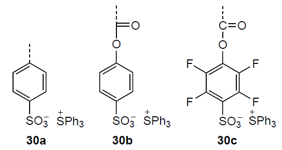
The introduction of PAGs into the polymer chain also improves the resist properties for post-lithography treatment, e.g., for reactive ion etching processes. Polymers 17 and 25a studied by Lee et al.[95] contained immobilized triphenylsulfonium salts with 4-(vinyl)benzenesulfonate (30a), 4-(methacryloxy)benzenesulfonate (30b), and 4-(methacryloxy)-2,3,5,6-tetrafluorobenzenesulfonate (30c) anions as PAGs. The authors elucidated the effects of the PAG amount and structure on the efficiency of reactive ion etching. It was shown that an increase in the PAG content correlates linearly with a decrease in the etching rate under model conditions for both silicon dioxide and polymer matrices. Resists based on PHS (17) had a higher etch resistance [the etching rate was 1 – 0.89 nm min–1 for various PAGs (30a–c) and various concentrations] than the acrylate-based resists containing γ-butyrolactone groups (1.32 – 0.99). It should be borne in mind that the nature of PAG is also important: fluorination and the presence of long ester linkers between PAG and the polymer matrix deteriorate the etch resistance of the materials; however, the introduction of fluorine into PAGs simultaneously markedly increases the acid quantum yield and the total sensitivity of the resist composition. Under real manufacturing conditions, this gain in sensitivity compensates for the above drawback.
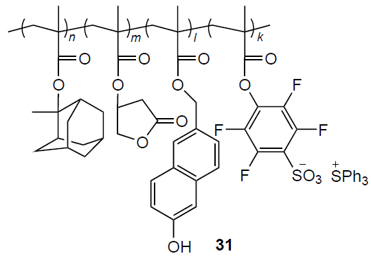
A successful example of a resist for EUV lithography is an acrylate matrix-based resist 31 with covalently bound PAG.[96][97] The resist had a sensitivity to EUV radiation of 12.7 mJ and the ability to form a pattern with a 22 nm half-pitch resolution, while exhibiting a wide exposure latitude. For various exposure power densities, LER was approximately 5 nm. By increasing the proportion of PAG, this value could be decreased to 3.1 nm. The limiting resolution of 17 nm half-pitch was achieved at a film thickness of 35 nm and a dose of 14.5 mJ.
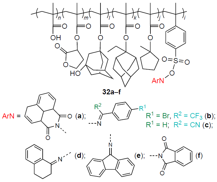
Liu et al.[98] synthesized and studied acrylate polymers with immobilized imido- and iminosulfonate PAGs 32a – f. The results of electron beam lithography show that these copolymers, in particular the resist based on 32c exhibit a resolution of 40 nm half-pitch at an electron beam dose of 73 mC cm–2. The sensitivity of these structures to EUV exposure was not investigated in this study.
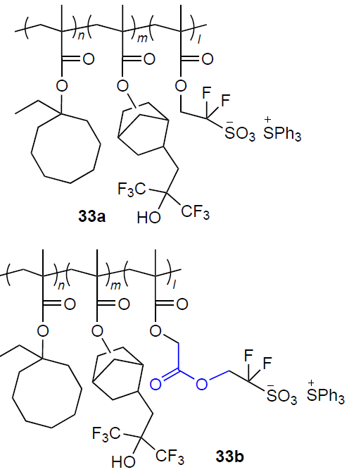
Maeda and co-workers[99][100] synthesized and studied resists with PAGs 33а,b (n = 40, m = 55, l = 5) immobilized into the acrylate matrix. Resists based on these structures showed the ability to form line-and-space patterns with a half-pitch of 36 nm, while possessing good sensitivity to EUV exposure: 9.45 mJ cm–2 for polymer matrix 33а and 10 mJ cm–2 for 33b.
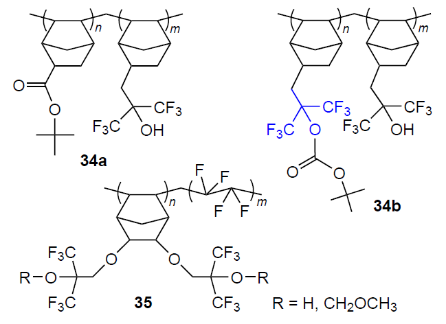
In 2000 – 2006, with the advent of F2 excimer lasers operating at 157 nm wavelength, the search for materials that are transparent in this range was initiated. The introduction of fluorine-containing groups proved to be the most practicable solution for the fabrication of polymer matrices for these resists; however, materials 34a,b (Refs [101-103]) and 35 (Refs [104][105]) proposed at that time had insufficiently high lithographic performance, which finally precluded further development of this topic. Although resists for 157 nm exposure wavelength have not been widely used, studies clearly demonstrated the efficiency of incorporating fluorine-containing groups into polymers and PAGs. Subsequently, these findings proved to be highly useful for the development of resists operating with other types of exposure such as EUV, which gave a new impetus to this research area.
Fedynyshyn et al.,[36] who evaluated the acid generation efficiency upon EUV exposure in various polymer systems of resists, found that the introduction of fluorine atoms has a considerable effect on the photoacid generation efficiency of the PAG used, that is, di(tert-butylphenyl)iodonium nonaflate, as it increases the polymer photosensitization. Resists based on fluoromethacrylates and fluoronorbornenes 36a – c had high absorption coefficients and Dill C parameters (Table 9). Thus, these results indicate the possibility of targeted modification of existing polymer matrices to adjust them to new exposure sources and manufacturing processes.
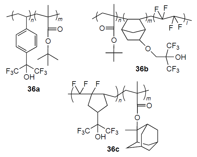
Thus, modification of resist components by introducing fluorinated derivatives is a potent tool for considerably enhancing the lithographic performance. As shown above in this Section, this approach is actively utilized in modern development of polymers with immobilized PAGs.
4.3.3. Resists based on peptoid structures
In 2021, Kaefer et al.,[106-108] reported a new class of photoresists based on peptoid polymers. These compounds are linear polymers 37a,b in which bonds are similar to the bonds between amino acids in proteins. Amide bonds in the polymer matrix can be cleaved by exposure to strong actinic radiation. The major process involves the homolytic cleavage of the C – N bond, which gives rise to two radicals.[109] The scission of the polymer backbone in the exposed areas leads to higher permeability of the matrix facilitating acid diffusion. In turn, this enhances the efficiency and completeness of deprotection in exposed areas.[106]
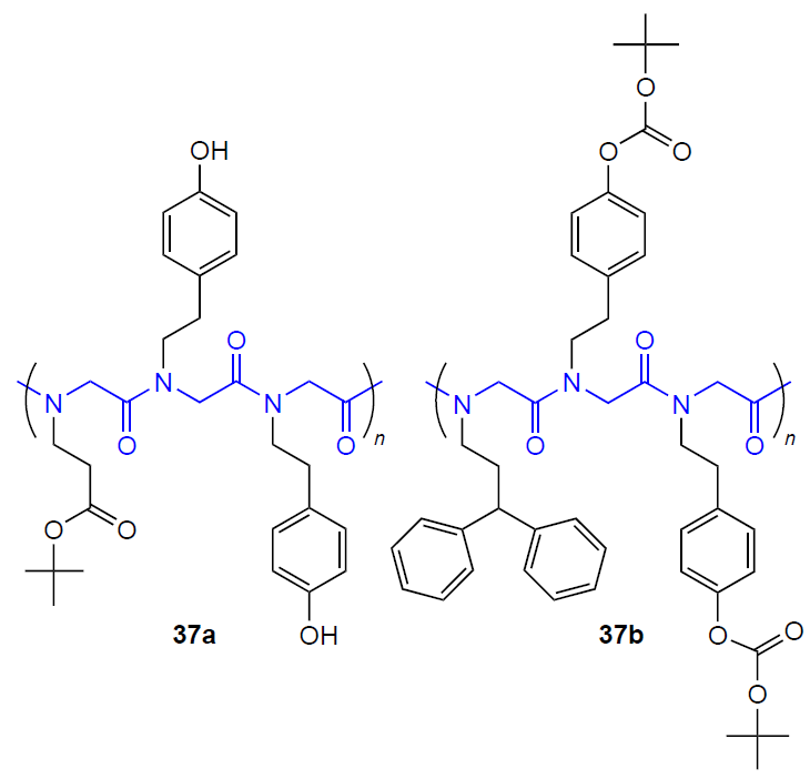
Meng et al.[107] synthesized polypeptoid structure 37a as a high-resolution polymer matrix for EUV resists. The polymer matrix was dissolved in 1-methoxy-2-propanol, with triphenylsulfonium nonaflate being used as PAG. A preliminary lithographic pattern was formed on DUV exposure at a dose of 100 mJ cm–2. Unfortunately, the preliminary pattern given in the paper does not allow one to assess the limiting characteristics of the resist. Subsequently, the polymer structure was complicated (37b) by using t-BOC-protected ethylamine and diphenylpropylamine as monomers.[105] The results obtained using EUV and electron beam lithography demonstrated the potential to achieve a resolution of down to 15 nm half-pitch for both types of exposure. The resist sensitivity to EUV radiation was 16 – 17 mJ.
4.4. Chemically amplified chain-scission positive resists
Chemically amplified resists in which the lithographic image formation is based on acid-catalyzed scission of the polymer chain have been studied as a highly sensitive alternative to resists based on the polarity switching mechanism. The key difference is that in this case, the resist solubility in the developer changes because of a decrease in the polymer average molecular weight upon the controlled bond cleavage in the polymer backbone under the action of photogenerated acid rather than because of chemical modification of the side groups.
Polyphthalaldehyde-based materials were among the first resists of this type to be studied. Although pure polyphthalaldehyde is thermally unstable at room temperature, it can be stabilized by acylation or alkylation of the terminal groups. The modified polymers retain stability at temperatures up to 250°C and can undergo acid-catalyzed depolymerization under the action of actinic radiation. Resists based on polyphthalaldehyde and triphenylsulfonium salts as PAGs are sensitive to UV radiation, X-rays, and ion beams. Sensitization of polyphthalaldehyde by onium salts as PAGs results in acid-catalyzed cleavage of acetal bonds in the polymer backbone and high sensitivity to EUV radiation (< 2.5 mJ cm–2).[65] Scheme 12 shows depolymerization of polyphthalaldehyde under the action of photoacid. The drawbacks of these resists include low thermal stability, low resistance to plasma etching, and intense outgassing accompanied by release of gaseous aldehyde, which contaminates the optical parts of the exposure equipment.
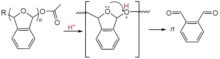
An increase in the thermal stability and decrease in the volatility of products can be achieved by introducing peripheral substituents. Wang et al.[110] compared polyphthalaldehyde with its derivatives substituted with chlorine, bromine, or trimethylsilyl group. According to thermogravimetric analysis data, all substituted polymers had higher thermal stability than the pristine compound. Indeed, the trimethylsilyl derivative underwent the lowest mass loss (1.1%) on heating to 160°C for 90 min, while the chlorinated derivative lost 3% of weight at 164°C after 44 min. The introduction of bulky substituents is the most effective way to stabilize the polymer chain and reduce thermal degradation.
Cyclic (39a) and linear (39e) brominated polyphthalaldehyde derivatives obtained by Deng et al.[44] also had a high thermal stability up to 178°С (glass transition temperature) exceeding that of unsubstituted linear derivatives (128°С). In combination with non-ionic PAGs 13a–c, these resists had a good sensitivity to EUV radiation (10 – 15 mJ cm–2).
Deng et al.[111] developed polyphthalaldehyde-based self-immolative polymers, particularly, brominated polyphthalaldehydes (39a – d) with covalently bound non-ionic PAG (10 mol.%). The resists based on these polymers had a sensitivity to EUV light in the range of 2 – 7 mJ cm–2. Despite the good sensitivity, the resists showed a moderate contrast; particularly for compound 39c, the contrast was 2.74.
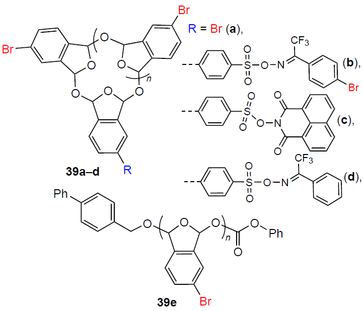
The plasma resistance of the resists based on polyphthalaldehydes can be increased in two ways:
(1) by the introduction of trimethylsilyl groups into the polymer;
(2) by mixing the polymers with novolac resins.
Both approaches are used to produce resists that can be dry-etched in a gas plasma.[110]
Linear and branched aromatic polyacetals can be used as resists for EUV lithography operating via chain scission reaction. The materials for electron beam and EUV lithography studied by Ober et al.[112] can serve as examples of polymer matrices for these resists. For example, polymer system 40 comprises acid-sensitive acetal groups in side chains and in the backbone, a rigid polyaromatic cage, and phenolic groups. The hydrophilicity of the polymers was varied by changing the degree of protection (R1 and R2 substituents). Cyclohexyl vinyl ether was used as a protecting group. Testing of resist samples based on these polymers showed that the optimal degree of protection is achieved when the content of protecting groups ranges from 0 to 30% of the total number of polymer units. The resist films were exposed to 13.5 nm wavelength radiation with increasing doses (0 – 14 mJ cm–2). The results showed a line-and-space pattern with 24 nm half-pitch resolution (30% protection) with an LWR of 8.1 and 22 nm half-pitch resolution (unprotected) with an LWR of 5.7 nm.
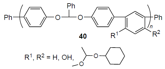
Cardineau et al.[113] synthesized tertiary aliphatic (41а) or cleavable tertiary benzyl esters (41b). Resists based on these polymers contained iodonium nonaflate as PAG, tetramethylammonium hydroxide as a base quencher, and ethyl lactate and PGMEA as solvents. A resist based on a cleavable tertiary benzyl ester had a maximum resolution of 40 nm half-pitch. Using this resist, a lower quality images with a resolution of down to 14 nm half-pitch were also obtained; however, in this case, the patterns had defects such as serpentine deformation and the formation of bridges between adjacent features. The authors attributed both defects to the high concentration of ether bonds in the polymer backbone, resulting in high swelling of the polymer matrix in alkaline aqueous developers and distortion of ultrasmall pattern features.
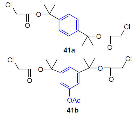
Iwashita et al.[114] prepared and studied two star-shaped (STAR) polymers 42a,b. The polymer architecture consisted of a core connected to arms by acid-cleavable bonds. The arms were formed by either 4-PHS (42a) or poly(4-hydroxy-α-methylstyrene) (PHOMS) (42b). Resists based on STAR polymers had better lithographic performance than their linear analogues in the formation of 30 nm half-pitch patterns (Table 10).
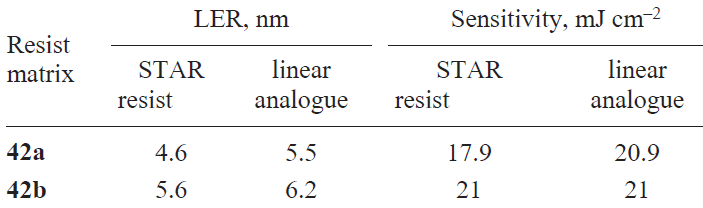
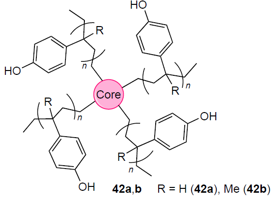
Thus, the STAR architecture decreases the line roughness for both types of polymers. The results demonstrate the potential for control of lithographic properties through the spatial structure, of the polymer rather than through the chemical composition alone.
4.5. Chemically amplified negative resists
Chemically amplified organic negative resists operate through intermolecular polymerization or cross-linking processes. In negative resists, the hydrophilic functional groups in the polymer are not protected, and, what is more important, molecules of cross-linking agents are added to the mixture. These molecules are either directly activated during the exposure or activated by the acid released in the exposed areas and form cross-links between various polymer chains during post-exposure bake. Thus, the exposed resist represents an insoluble polymer network. During the development, the resist is treated with an aqueous solution of a developer to remove the unexposed areas. It should be noted that negative tone resists with direct photoactivation of cross-linking agents are typically used in photolithography at 365 nm.[115] However, there are also reported examples of successful use of chemically amplified negative resists in the EUV lithography.
Epoxy functional groups are used most often in these resist formulations. The generated photoacid catalyzes epoxide ring opening, leading to the formation of highly reactive carbocations. These active sites initiate intermolecular polymerization reaction. As a result, a three-dimensional cross-linked network insoluble in the organic developer is formed in the exposed area (Scheme 13).
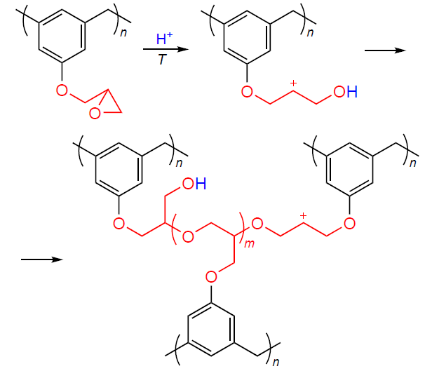
An example of commercially available resist based on epoxy cross-linking of bisphenol A is SU-8, which was developed and patented by IBM in 1989 and is currently manufactured by Shell Chemicals under the trade name EPON SU-8.[116] The EPON SU-8 photoresist is used to form three-dimensional structures with a high aspect ratio by deep X-ray (LIGA) and DUV lithography.[117-119] This photoresist can form up to 3 mm thick layers (using the spin-coating method), which makes it a key material for the fabrication of complex 3D microstructures.[120] The primary formulation of the SU-8 photoresist includes: epoxidized polymer with epoxy side groups 43, triarylsulfonium hexafluoroantimonate 44а,b as PAG, and γ-butyrolactone as a solvent. Additives may be used to modify the properties, e.g., polymer modifiers to control flexibility, strength, and adhesion; fillers; plasticizers; pigments; and rheological additives.[118]
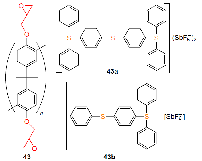
Pillars with a diameter of 8 μm were obtained in a 480 μm-thick layer by X-ray lithography using radiation in the 7 – 12 Å wavelength range; the roughness of the pillar walls was less than 0.2 μm and the verticality was nearly perfect.[121] The sensitivity of the 25 μm-thick SU8 resist to X-rays was 2500 mJ cm–2.[122]
Despite the unique possibility of forming high-aspect-ratio 3D structures, the research techniques involving SU-8 are unsuitable for mass industrial production. The key limitations are high cost of the processes (equipment, exposure) and low throughput.[120]
Apart from epoxy groups, other oxygen-containing aliphatic rings can also act as cross-linking agents. Park et al.[123] reported resists for EUV lithography based on polymerized 2-[2-(4-vinylphenoxy)ethyl]-[1,3]-dioxane 45. The sensitivity of these resists to 248 nm DUV radiation was found to be moderate: 150 mJ cm–2.
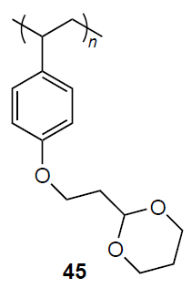
The main drawback of the cross-linking negative resists is film swelling during the development, which markedly limits the resolution. This phenomenon arises when an organic solvent, the developer, penetrates into the 3D cross-linked polymer network and causes its expansion, which leads to distortion of the lithographic pattern.
One way to address this problem is the addition of epoxy novolac resins to the resist. This approach was implemented for the resists used in electron beam lithography.[124][125] Compared with the original formulation, swelling was virtually eliminated. The resist provided a resolution of 100 nm.
4.6. Photosensitized chemically amplified resists
Photosensitized chemically amplified resists (PSCAR) are similar in their primary composition to polymer-based chemically amplified resists and include a protected polymer, PAG, and a quencher. A key distinction is the presence of an additional component, a photosensitizer precursor. This precursor contains an acid-sensitive ketal protecting group, which is hydrolyzed in the presence of photogenerated acid to form a ketone that acts as a photosensitizer. Benzophenone derivatives are most commonly used as precursors (Scheme 14).
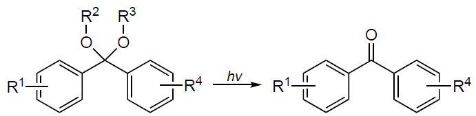
The lithography process using PSCAR (Fig. 4) includes an additional stage of exposure to UV radiation to increase the sensitivity. On exposure to EUV radiation, PAG generates a photoacid. The released acid reacts not only with the polymer matrix to remove the protecting groups, but also with the photosensitizer precursor to convert the ketal to a ketone. During the additional stage of UV exposure at 365 nm, an acid is generated through the action of the photosensitizer, and the amount of the acid in the initially exposed areas increases, which in turn increases the degree of polymer deprotection. The increase in the acid amount necessitates more stringent control of diffusion; therefore, to achieve the same critical feature size, a larger amount of base quencher is used in PSCAR resists.[126-128] Lines with a 16 nm pitch were obtained by EUV lithography at exposure doses of 15 – 30 mJ cm–2 and LWR of 4.3 nm.
![[{"id":"oo2b9DHO95","type":"paragraph","data":{"text":"Sequence of lithography stages using photosensitized chemically amplified resists"}}]](/storage/images/resized/dYnzDo6BLudHgzmS0nkTXVaSJ0UuUVnfV5nkFobr_xl.webp)
5. Organic non-chemically amplified resists
The composition of non-chemically amplified resists for EUV and DUV lithography is much simpler than the composition of chemically amplified resists. As a rule, the resist matrix already contains a light-sensitive component; therefore, the resist operation does not require the addition of PAGs and, hence, does not require components for the control of acid diffusion.
Non-chemically amplified resists used in DUV and EUV lithography are, most often, positive (in this review, negative resists are also considered). Their operation is based on two key mechanisms of image formation: polymer chain scission and polarity switching reactions.
5.1. Polymer chain-scission resists
A widely used resist material for electron beam lithography, polymethyl methacrylate (PMMA), is used as an EUV resist. On exposure to high-energy photons from electron beam or EUV radiation, PMMA undergoes random chain scission, which gives rise to low-molecular-weight fragments and generates a solubility contrast (Scheme 15). Higher molecular weight PMMA is better suited for EUV lithography in terms of LER, but PMMA-based resists are also used for X-ray lithography.[129][130] As a rule, the conditions of resist deposition and development do not change depending on the type of radiation used for exposure. However, PMMA resists have relatively low sensitivity to both EUV and X-ray radiation (Table 11).
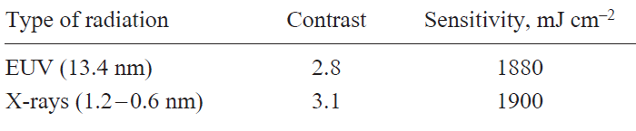
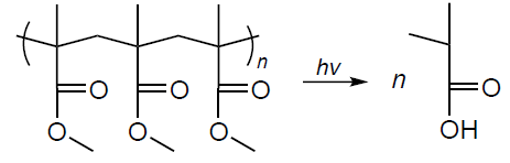
It is worth noting that these values were obtained for a 350-nm-thick PMMA film; when working with films with a thickness of 100 nm or less, the sensitivity is usually higher. Thorough selection of development and post-exposure bake conditions for PMMA makes it possible to control the feature line edge roughness.[131] Out of three solvent systems tested for the development, that is, methyl isobutyl ketone (MIBK); MIBK/isopropyl alcohol (IPA) (1 : 3); and GG developer,* the lowest roughness characteristics were achieved by using the GG system. However, this advantage was accompanied by a threefold increase in the development time compared to that for MIBK/IPA. The use of ultrasound reduced the time of development, but even in this case, it amounted to 12 min for GG and only 4 min for the MIBK/IPA system. Despite the pronounced increase in the duration of the process, which affects the throughput of manufacturing, this drawback is counterbalanced by the substantial decrease in roughness:
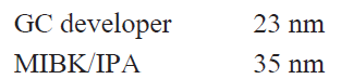
Thus, the choice of developer for PMMA resist is an engineering trade-off between the throughput (development time) and quality (edge roughness) or sensitivity (the higher the MIBK content in the system, the slower the development rate and the higher the sensitivity; however, the quality of lithography decreases).
Bulgakova et al.,[132] who exposed a 160 nm-thick PMMA layer to EUV radiation, found the following dependence of the sensitivity and contrast on the developer nature:
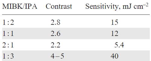
Nazmov et al.[133] compared the X-ray lithography performance of the SU-8 and PMMA resists. On exposure to X-rays, the lithographic images were formed with the same resolution for both resists; however, as expected, SU-8 surpassed PMMA in the radiation and mechanical strength of the formed structures.
Thus, the main drawbacks of PMMA-based EUV resists are as follows:
— low resistance to dry etching,
— low sensitivity,
— the dependence of the lithographic quality on the nature of the organic solvents used for the development,
— a large amount of released gas.
Lithographic performance of PMMA resists can be enhanced by chemical modification, particularly, by introducing electron-withdrawing substituents and aromatic groups. As an example, consider the ZEP520A[134] and mr-PosEBR resists for electron beam lithography, which contain chlorine and aromatic groups. Both resists demonstrated excellent sensitivity to EUV radiation:

Using both resists, line-and-space patterns with a resolution of about 25 nm were formed. A higher quality of the pattern was achieved for ZEP520A.[135]
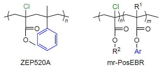
Copolymerization of methyl methacrylate (ММА) with various monomers such as methacrylic acid (MAA), methacrylonitrile (MAN), butyl acrylate (BA), heptafluoroisobutyl methacrylate (HFIBMA), tetrafluoropropyl α-chloroacrylate (TFPCA), and octyl α-cyanoacrylate (OCA) considerably enhances the resist properties.[131] On exposure to radiation at 13 nm wavelength, the resulting copolymers exhibited higher sensitivity compared to the original PMMA; however, they generally provided a moderate contrast (Table 12). Copolymers with methacrylonitrile proved to be not only highly sensitive, but also resistant to plasma-chemical etching.
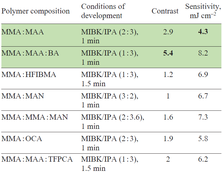
Modified polysulfones 46, which contain PMMA chains as side substituents, can be conventionally classified as PMMA-based resists. These non-chemically amplified resists are successfully used in immersion lithography at a wavelength of 193 nm.[136][137] On exposure to EUV radiation, polymer backbone scission takes place to give smaller fragments; this makes it possible to form an image. The PMMA side chains remain largely intact due to their high strength and stability and form a residual polymer network that provides the structural matrix for the patterned features after exposure.[136][137] Resists based on polymers containing 10 mol.% PMMA segments with a molecular weight of 2700 Da demonstrated a maximum resolution of 22.5 nm. A slight increase in the sensitivity compared to poly(1-pentene sulfone) was also observed, being in some cases accompanied by a decrease in roughness (Table 13).[136]
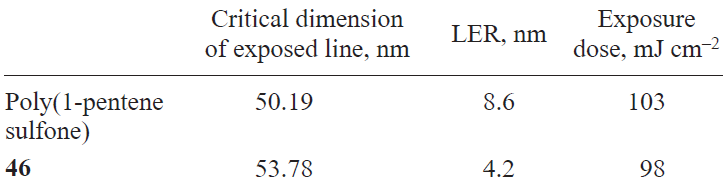
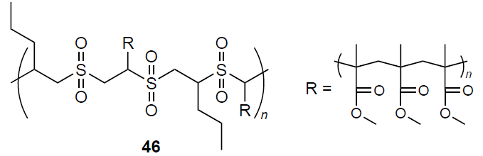
Whittaker and co-workers[138][139] studied poly(norbornene sulfone)-based resists 47a – d. These materials were developed for immersion lithography at 193 nm wavelength. The resist sensitivity was approximately 50 mJ cm–2. Line-and-space patterns with 60 and 120 nm half-pitches were obtained. However, the resulting images had a large number of bridge defects (Fig. 5) and high roughness, which casts doubt on the expediency of further research along this line.
![[{"id":"wi01Zerkt6","type":"paragraph","data":{"text":"SEM images of the results of lithography with 120 nm resolution for poly(norbornene sulfone)-based resists shown at various magnifications: (<i>a</i>) 10-fold, (<i>b</i>) 50-fold.<sup>139</sup> ©SPIE Proceedings, 2010."}}]](/storage/images/resized/j6NJ47YVh2dmVKYthK72GHU6KvSgXdkeFrpqiZRg_xl.webp)
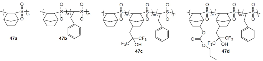
Whittaker et al.[137] synthesized and studied star-shaped polycarbonates consisting of EUV-sensitive carbonate moieties and alicyclic groups, which provided high glass transition temperatures and good etch resistance. Preliminary studies on resist exposure demonstrated the possibility of forming a lithographic image with 50 nm resolution. However, there is some distortion in the line shape in the exposed image, which is apparently due to polymer swelling during development in a solvent (Fig. 6).
![[{"id":"t87MEq8kEY","type":"paragraph","data":{"text":"SEM image of lithography with 50 nm resolution.<sup>137</sup> ©SPIE Proceedings, 2009."}}]](/storage/images/resized/N7pxH0Qq3pixLYC0vr4VdYJ4bT6bIW5JbdgJvIz2_xl.webp)
* GG is a standard developer used in the LIGA (Lithographie, Galvanoformung, Abformung) process representing a system of 2-butoxyethoxyethanol, morpholine, 2-aminoethanol, and water.
‡ Exposure dose (D50) is a dose at which the residual resist thickness is 50% of the initial one. In this experiment, the initial film thickness was 80 nm, and D50 corresponded to a residual thickness of 40 nm.
5.2. Polarity switching resists
Resists operating via the polarity switching mechanism have been developed on the basis of polysulfones. The effect is achieved by introducing o-nitrobenzylnorbornenecarboxylate side group into the polymer. This group undergoes photochemical cleavage to give a carboxylic acid, which endows the polymer with good solubility in weakly alkaline aqueous solutions (Scheme 16). The presence of norbornene moieties increases the etch resistance of the polymer. The resists were tested using DUV (193 nm) and electron beam lithography. The electron beam exposure resulted in patterns with a resolution of 32 nm comparable to those of the PMMA-based resist. The resist sensitivity to exposure at 193 nm was increased by the additional introduction of acridine (15 mass % relative to the polymer mass) as a sensitizer. Lines and spaces with 150 nm resolution were obtained using exposure dose of 170 mJ cm–2.[140]
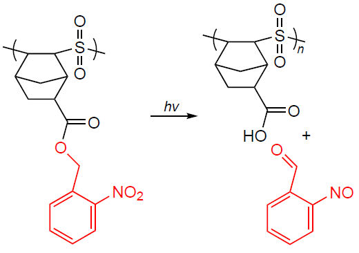
Non-chemically amplified polarity switching negative resists were reported by Gonsalves and co-workers.[141][142] EUV-sensitive polymers 48a – d were prepared by polymerization of (4-(methacryloyloxy)phenyl)dimethylsulfonium triflate with isopropyl methacrylate, methyl methacrylate, 4-carboxystyrene, or N-vinylcarbazole. On exposure to EUV radiation with an energy of 103.5 eV, the triflate and the ester group degrade to give off the SO2+, SO+, and CF3+ groups. Thus, on exposure to radiation, the sulfonium group soluble in aqueous solutions is converted to a less soluble sulfide group (Scheme 17). Resists based on the homopolymer of (4-(methacryloyloxy)phenyl)dimethylsulfonium triflate and its copolymer with methyl methacrylate 48b had 20 nm resolution in the electron beam lithography.
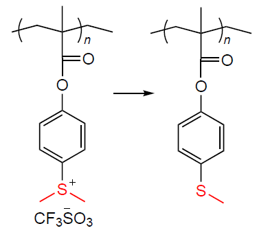
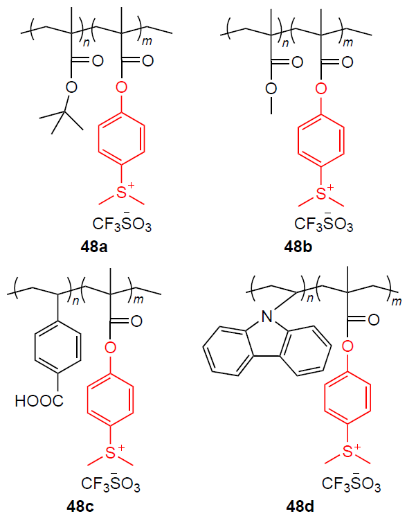
A resist based on copolymer 48a of (4-(methacryloyloxy)phenyl)dimethylsulfonium triflate with isopropyl methacrylate was tested by EUV lithography and had a sensitivity of 26.64 mJ cm–2 for 20 nm half-pitch line patterns.
6. Molecular glass-based resists
Molecular glasses are organic compounds consisting of complex molecules with a relatively small size (up to 1 nm) and moderate molecular weights (usually not exceeding 2000 atomic mass units), which are capable of forming amorphous films. Due to their small molecular size, they are promising materials for the formation of resists with a low line edge roughness. The typical structure of a molecular resist comprises a multifunctional molecule containing a central core responsible for the glass transition temperature and etch resistance, and peripheral functional groups that regulate hydrophilicity, adhesion to the substrate, and photosensitivity. The glass transition temperature is a critical parameter, because the material should retain the thermal stability and amorphous state throughout all stages of the post-exposure treatment.[143]
Polyphenols are among the most extensively studied compounds used to obtain molecular resists. To date, a vast number of diverse polyphenolic structures have been synthesized. Although there is no versatile structural platform for polyphenol-based resists, one of the most studied structures is compound 49 reported by Shiono et al.[144-147] These polyphenolic derivatives were originally developed for electron beam lithography; however, subsequently they also proved to be promising for EUV lithography.
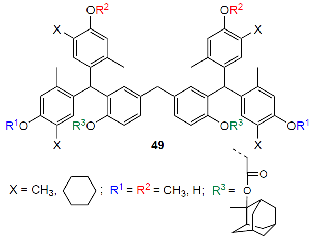
Resists based on polyphenol 49 (Х = CH3; R1 = R2 = H; R3 = 2-methyl-2-adamantyl acrylate) were tested by EUV lithography in two compositions, one being chemically amplified and containing PAG and the other containing no PAG.[145][146] Both types of resist had comparable resolution and LER characteristics: the resolution of non-chemically amplified resist was 28 nm at an exposure dose of 12.2 mJ cm–2, while LER was very low (3.6 for 45 nm line-and-space patterns).[145][146]
The polyphenolic negative resist based on compound 50 on exposure to EUV radiation showed 29 nm resolution at an exposure dose of 12 mJ cm–2; lines with 28 nm half-pitch were obtained; however, the lithographic pattern had numerous defects.[148]
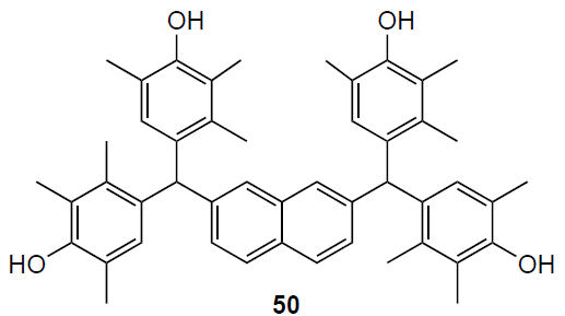
Compounds based on xanthenediol 51 can also be classified as molecular resists.[149] A negative resist made of this compound contained hexamethoxymethylmelamine as the cross-linking agent, sulfonium sulfonate as PAG, and a quencher. The resist exhibited good sensitivity to both EUV radiation and electron beam. In both cases, 20 nm half-pitch line-and-space pattern was formed. The exposure dose was 44 mC cm–2 for electron beam lithography and 60 – 80 mJ cm–2 for EUV.
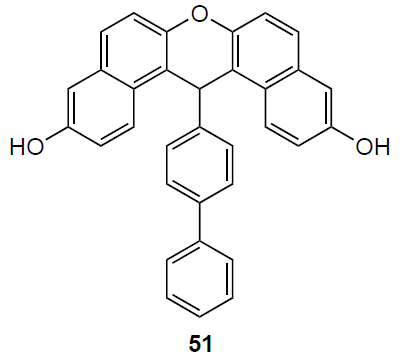
Compounds based on calixarene such as C-(4-tert-butylphenyl)calix[4]resorcinarene represent another class of molecular resists. Calixarenes are cyclic compounds containing a number of repeating units; in this respect, they resemble polymers, but they have well-defined structures. It was established that several calixarene derivatives are molecular glasses with a number of appropriate properties, including a high glass transition temperature. These materials were first proposed as negative resists for lithography in 1996 by Fujita et al.[19] The calixarene molecule is about 1 nm in size. Despite their low sensitivity, owing to the small size, they can provide a resolution of less than 10 nm. Calixarene films are transparent at 300 nm, which makes it possible to use this material in i-line lithography (UV radiation at 365 nm wavelength). In addition, the absorbance of calixarenes at 248 nm is 0.3 μm–1; therefore, they can be used in lithography using a KrF excimer laser.[19] Calixarene-based resists for electron beam lithography have also been proposed.[150]
There are examples of successful use of calixarenes in EUV lithography. Kudo et al.[151] reported positive resists based on hyperbranched polyacetals with C-(4-tert-butylphenyl)calix[4]resorcinarene (52) molecules as branching points. The polymers were synthesized by polycondensation of C-(4-tert-butylphenyl)calix[4]resorcinarene with 1,4-bis(vinyloxy)cyclohexane (53а), 1,3-bis(vinyloxy)propane (53b), 1,3,5-tris(vinyloxy)cyclohexane (53c), 1,5-bis(vinyloxy)-3-oxapentane (53d), and 4,4'-bis(vinyloxy)-1,1'-bicyclohexane (53e). The resulting polymers had good solubility, film-forming properties, and thermal stability. The resorcinarene copolymer with 1,4-bis(4-vinyloxy)cyclohexane (53a) in the presence of a triphenylsulfonium salt as PAG showed the highest sensitivity to EUV radiation (1.0 mJ cm–2). The sensitivity of other compositions did not exceed 10 mJ cm–2. A study of the etch resistance of the polymer films in CF4 plasma revealed a high etch resistance comparable to that found for PHS resins.
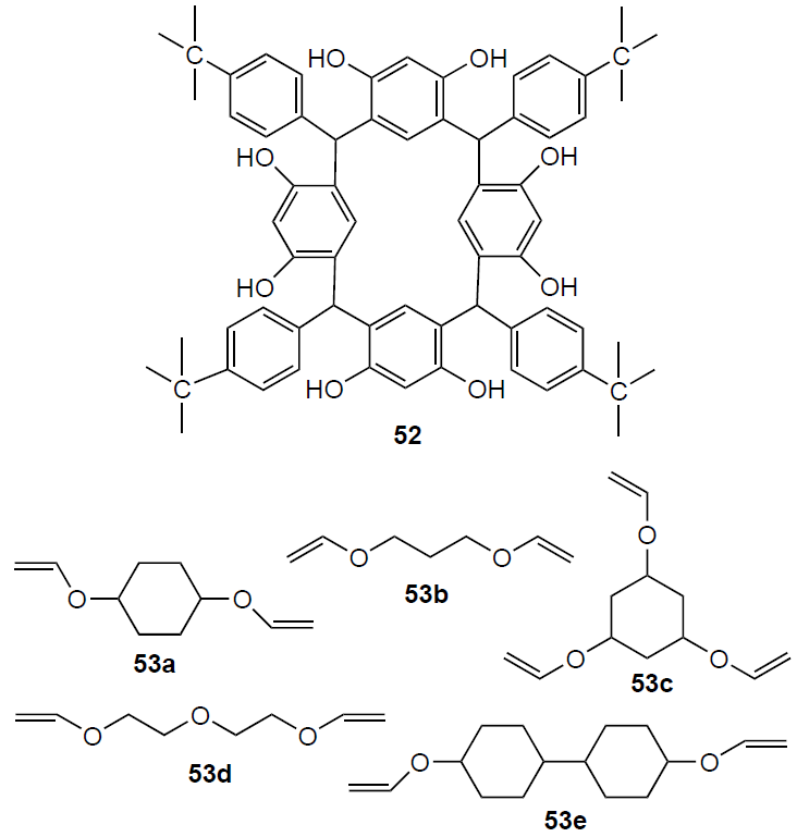
Dow Electronics has developed several positive molecular glass resists based on calixarene cores (54) with acetal leaving groups. The resists formed amorphous films and exhibited good contrast and lithographic pattern quality on exposure to DUV radiation (248 nm).[152] The resist sensitivity to EUV radiation also proved to be high (6.6 mJ cm–2). Line-and-space patterns with 28 nm half-pitch were formed. However, at this resolution, bridge defects were observed in the image, and LER was 5.6 nm, which exceeds the value for the reference resist (3.7 nm). These drawbacks can be attributed to the non-uniformity of PAG distribution, which induces film delamination.[152]
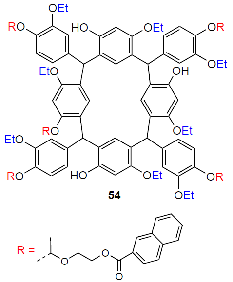
Apart from positive tone resists, calixarenes can also be used to fabricate negative tone resists.[148] A resist based on phenylcalix[4]resorcinarene 55 showed a sensitivity of 14.8 mJ cm–2 and a resolution of 29 nm half-pitch.
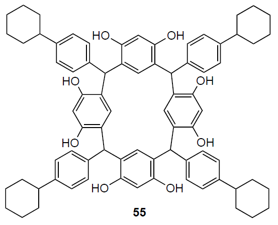
A compound structurally similar to calixarenes is noria that is obtained by the acid-catalyzed condensation of resorcinol with 1,5-pentanedial.[153][154] The noria molecule 56 (R = H) is based on calix[4]resorcinarene and represents a double cyclic oligomer with ladder bonds between the two rings that form a more rigid structure than calixarene.
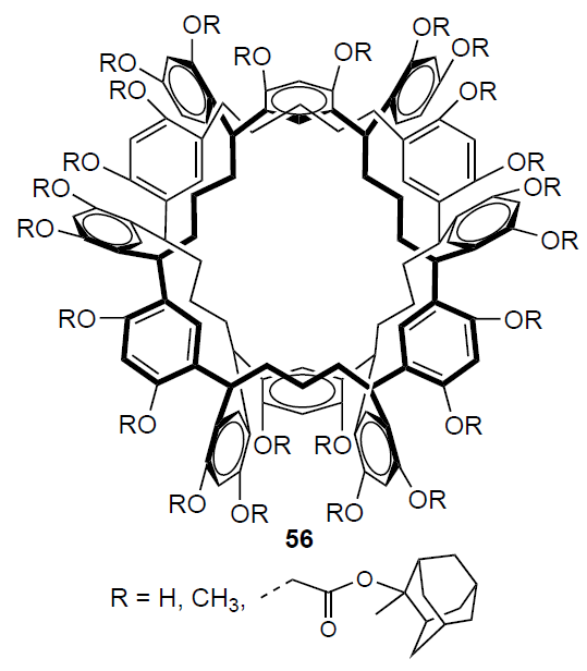
Polarity switching positive resists have been synthesized using modified noria derivatives with 2-methyl-2-adamantyl acrylate side groups (56).[154][155] The noria molecule with adamantyl groups is insoluble in aqueous solutions of bases, whereas a molecule without these groups is readily soluble [2.5 mass % solution of (Me4N)+OH–]. The obtained resists were able to form a high-resolution pattern. Kudo et al.[154] obtained resists based on the noria molecule with different degrees of adamantyl substitution and with triphenylsulfonium triflate as PAG. In the obtained noria molecules, 11%, 18%, 45%, 53%, or 75% of hydroxyl groups were replaced by adamantyl groups. A comparison of molecules with 18% and 53% protection under EUV exposure showed that the number of adamantyl groups affects the quality of the lithographic pattern. A smaller number of adamantyl groups decreases LER and slightly decreases the exposure dose (Table 14).
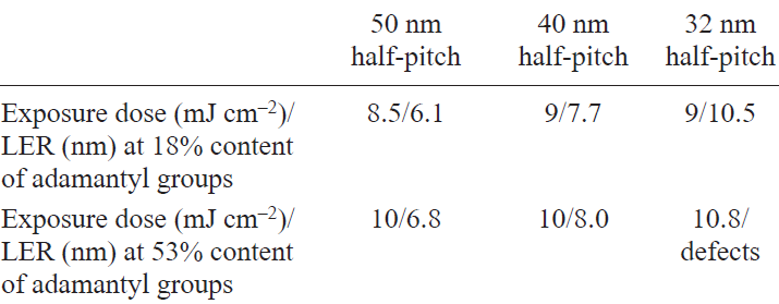
Using noria molecules, it is possible to obtain not only positive, but also negative tone resists. Kulshreshtha et al.[156][157] produced a resist based on the noria molecule with oxetane substituents, which acted as cross-linking agents in the acid catalysis. Triphenylsulfonium triflate was used as PAG and trioctylamine served as a quencher. The best resolution was achieved for resists based on noria molecules containing 5% and 20% oxetane groups. The resists were used to form less than 20 nm half-pitch patterns (Fig. 7) using exposure dose of 37.9 mJ cm–2 and LER of 4.2 nm.
![[{"id":"RDRCqYm-KP","type":"paragraph","data":{"text":"SEM image of lithographic lines with 20 nm half-pitch for a resist based on the noria molecule with oxetane substituents.<sup>157</sup> © Nanotechnology, 2014."}}]](/storage/images/resized/2GXxeamvbvv17cJri8Hf0OqtR1ZuAFxamh9PQheE_xl.webp)
Fullerene C60 derivatives (57) can be used to produce molecular resists. The small diameter of C60 molecule equal to 0.7 nm makes it a potential material for high-resolution lithography. Resists based on C60 and its derivatives are used as negative tone resists for electron beam lithography.[158][159] A C60-based resist decreases the dissolution rate in a developer due to fragmentation of the C60 molecule on exposure to electron beam. These compounds exhibit good resistance to plasma chemical etching, and resists based on them show promise for EUV lithography.
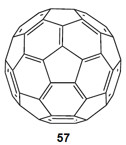
Chemically amplified negative tone resists have been developed using fullerene derivatives. Frommhold et al.[160][161] reported resists comprising fullerene derivatives, a cross-linking agent, and PAG. The resist exhibited high resolution (20 nm half-pitch) for an exposure dose of 20.3 mJ cm–2, LER of 5.65 nm. Later, the authors achieved 16 nm resolution; however, for this resolution, the line pattern was distorted, which was attributed to swelling during exposure. Apart from the usual factors affecting the quality of lithography, i.e., PAG and quencher concentrations, the dependence of contrast and LER on the total concentration of the resist components was found. The best image with 16 nm half-pitch was obtained at a total component concentration of 15 mass %. The nature of the developer also has a pronounced effect, first of all, on the LER values (Table 15).
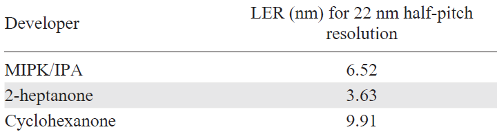
A new type of molecular resist called multi-trigger resists has been proposed.[162-165] 1,8-Diazabicycloundec-7-ene was allowed to react with tert-butyl (4-(2-hydroxyethyl)phenyl) carbonate. The authors were unable to confirm the structure of the reaction product; three possible structures for the final product were proposed, of which compound 58a was chosen as the most likely. A negative tone resist for EUV and electron beam lithography was formed using this compound in combination with a triphenylsulfonium salt as PAG and tris(4-hydroxyphenyl)methane triglycidyl ether 58b as a cross-linking agent. Using EUV exposure, lithographic patterns with half-pitches of 32 nm (30 mJ cm–2, LER of 2.15 nm) and 28 nm (35 mJ cm–2, LER of 3.2 nm) were obtained. A 22 nm half-pitch pattern was obtained at an exposure dose of approximately 50 mJ cm–2, but the image had defects.
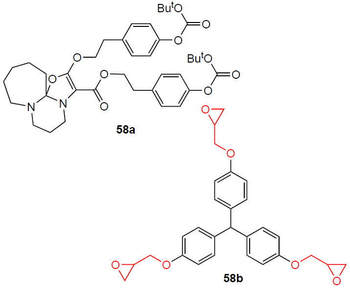
The variation of the nature and amount of the base quencher (various triphenylsulfonium salts) made it possible to improve LWR of this resist to 3.56 nm for a half-pitch of 14 nm.[166] Plasma etching showed that the etch resistance of this material was comparable to that of high-durability commercial electron beam SAL601 resist.[167] The authors called their system a multi-trigger resist. The operating principle of this material is similar to that of a chemically amplified resist. The released acid molecules act on several active sites. In the presented resist system, these are the t-BOC protecting groups of the 1,8-diazabicycloundecen-7-ene derivative and the epoxy groups of the cross-linking agent. In the areas with a large number of activated PAG molecules (areas with high exposure doses, e.g., the centre of a pattern feature), the resist components are activated in close proximity to one another, resulting in PAG regeneration; thus, the reaction chain propagates, providing a high sensitivity. In the areas with a small number of activated PAG molecules (areas with low exposure doses such as edges of a pattern feature), the activated resist components are too far from one another to react, and PAG molecules are not regenerated and are thus removed from the reaction, and the reaction is terminated. As a result of this mechanism, the multi-trigger resist increases the concentration of activated PAG in the edge regions of the exposed features and reduces the undesirable acid diffusion from these regions.[163][164]
Manouras and Argitis[162] reported non-chemically amplified molecular resists for DUV lithography based on deoxycholic acid 59 and 9,9-bis-4-hydroxyphenylfluorene derivative 60. The operation of these resists is based on the polarity shifting mechanism in which the o-nitrophenyl is the leaving group in the photoreaction. It was found that the resist based on compound 60 is more sensitive to DUV radiation than the deoxycholic acid-based one.
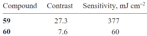
The addition of 20 mass % calixarene as a dissolution catalyst to the resist based on compound 60 improved the performance: the contrast increased to 10 and the sensitivity decreased to 8.3 mJ cm–2.
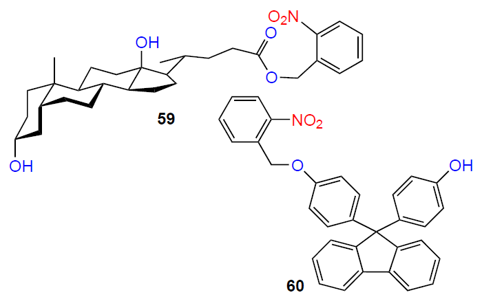
7. Silicon-based resists
Silicon-based resists can be conventionally subdivided into two groups, those based on organic polymer compounds containing silanes and siloxanes as functional groups and moieties[168] and those based on silsesquioxanes, including hydrogen silsesquioxane (HSQ) 61.[169] Most silicon-based resists are used in electron beam lithography. However, silicon-based resists may also have considerable potential for EUV and X-ray lithography, since silicon-containing functional groups are sensitive not only to electron beams but also to X-rays.
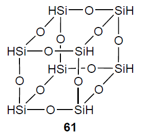
Currently, HSQ-based resists are the most extensively studied class of silicon negative resists for electron beam lithography. HSQ is a silicon compound with the formula (HSiO3/2)8; the lattice structure is cubic, with silicon atoms being located at the corners of the cube and oxygen atoms being on the edges. On exposure to electron beam or radiation, HSQ molecules begin to cross-link to give intermolecular Si – O – Si bonds; this results in a structure similar to amorphous silica. Rathore et al.[170] described two mechanisms of cross-linking of HSQ molecules. The first one is dehydrogenation involving the formation of intermolecular Si – Si silane bonds with the release of molecular hydrogen. The second mechanism involves cleavage of the intramolecular siloxane bonds and formation of intermolecular siloxane bonds (Fig. 8).[171][172]
![[{"id":"9edRFpGTeN","type":"paragraph","data":{"text":"Mechanisms of degradation of HSQ molecule on exposure to electron beam or EUV radiation.<sup>170</sup> © ACS Applied Materials & Interfaces, 2021."}}]](/storage/images/resized/AtmFMHBvPIDYYN1aw0H22rtJShQwmcxx7rj97qmX_xl.webp)
An HSQ-based resist exhibits high resolution and selectivity to plasma chemical and reactive ion etching.[173][174] Currently, the HSQ resist is among the promising electron beam resists due to low LER, high etch resistance, and small molecular size. Therefore, most publications are devoted to the use of this resist in the electron beam lithography;[175-181] using various development procedures, up to 10 nm wide lines with 30 nm half-pitch[182] and up to 5 nm wide lines[183] have been obtained.
In EUV lithography, the HSQ resist also shows good resolution and good sensitivity. Junarsa et al.[184] compared the lithographic performance of the resists based on HSQ and PMMA and two commercial chemically amplified resists on exposure to radiation at 13.5 nm wavelength. The EUV sensitivity and contrast of HSQ resist were 11.5 mJ cm–2 and 1.64, respectively. Despite the low contrast, which is markedly lower than that of chemically amplified resists, but somewhat higher than that of PMMA resists, the HSQ resist had lower LER values than the PMMA reference resist in a pattern of 40 nm wide lines:
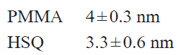
Wachulak et al.[185] exposed the HSQ resist to a tabletop EUV laser operating at 46.9 nm wavelength. The authors produced dense arrays of nanoholes and nanodots with a modulation depth of approximately 100 nm. It was found that the sensitivity of the HSQ resist at this wavelength is about 14 mJ cm–2. The penetration depth of the radiation was approximately 150 nm, which is almost an order of magnitude greater than that for PMMA resist at this wavelength.
Rantala and co-workers[186][187] described inorganic resists based on the products of controlled hydrolysis of organosilanes. They obtained compounds with different molecular weights: 3000 and 5000 a.m.u. Unfortunately, the authors did not specify the exact structure of the products. The synthesis products were dissolved in methyl isobutyl ketone. The resists were tested by electron beam and EUV lithography. The resists had low LWR (< 2 nm), a relatively high sensitivity (40 – 60 mJ cm–2), excellent etch selectivity, and patterning upon post-exposure development in aqueous solutions of (Me4N)+OH–, which is commonly used in industry. A study of the effect of etching and pre-exposure bake temperature on the quality of the lithographic image showed that the obtained silicon compounds can be used without pre-exposure bake, which considerably simplifies the lithographic process.
Mojarad et al.[188] compared three resists (HSQ, organic chemically amplified, and inorganic resists) on exposure to EUV radiation and soft X-ray radiation at 6.5 nm wavelength. Using EUV lithography, lines with 18 nm half-pitch were formed; an equivalent resolution could not be achieved for exposure to 6.5 nm: the minimum half-pitch value was 22 nm. In both cases, the HSQ resist had better LER values (< 2 nm).
Ali et al.[189][190] investigated chemically amplified resists prepared by polymerization of five various acrylates: tert-butyl methacrylate, methyl methacrylate, methacrylic acid, polyhedral oligomeric silsesquioxane (POSS)-propyl methacrylate 62а,[191] and PAG incorporated directly into the polymer chain 62b. Under EUV radiation, the resist demonstrated high sensitivity of 1 – 1.5 mJ cm–2 compared to existing commercial resists, while exhibiting a satisfactory contrast of 3. Apart from EUV radiation, the material was exposed to X-rays at 1 nm wavelength; the resist sensitivity was 60 – 80 mJ cm–2, while the contrast was 4.8. The required dose of X-ray radiation turned out to be much higher than that required for EUV exposure, due to the very low absorption coefficient in the X-ray range. The percentage of PAG in these resists ranged from 15 to 4.3 mass %, indicating that the resist sensitivity can be adjusted by varying the PAG content.
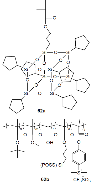
From a synthetic standpoint, one of the simplest methods for the preparation of silicon-based resists is to incorporate silane or siloxane groups into polymers such as PMMA. Bulgakova et al.[192] prepared polymers incorporating chemically diverse disilanes. It was found that disilane-modified PMMA samples had a higher sensitivity to Х-ray radiation (44 Å) and better contrast than non-modified PMMA. The sensitivity of non-modified PMMA was 670 – 600 mJ cm–2 for this type of exposure, whereas for modified PMMA, it ranged from 275 to 120 mJ cm–2 depending on the structure; the contrast for all samples was 6, which is markedly higher than that of some commercial resists.
8. Metal-based resists
Most resists for EUV lithography based on metal organic compounds and metal complexes are negative tone resists. The development of these resists is based on incorporation of Hf, Zr, Zn, and Sn atoms, which enhance the generation of photoelectrons on exposure to EUV radiation. In the case of an inorganic photoresist, the composition of the inorganic core determines the X-ray absorption coefficient, while the type of organic ligands on the core surface determines the photochemical transformation of the resist that occurs after exposure. Thus, new inorganic photoresists with specified properties are being developed along two lines, one involving variation of the composition and structure of the major inorganic component and the other involving variation of the nature of organic ligands on the surface of the inorganic core. As a rule, the small core size of these resists also promotes a decrease in LER. In addition, if an appropriate metal has been chosen, incorporation of the metal into the resist can provide other benefits such as higher etch resistance compared to that of organic resists. The increase in the etch resistance makes it possible to use thin resist layers (down to 20 nm), which is a potential advantage for the lithography production processes.[115]
Fallica et al.[193] performed a comparison of the EUV absorption coefficients of twelve resists, including PMMA resists, HSQ resists, organic chemically amplified resists, organic non-chemically amplified resists, and Inpria metal oxide-based inorganic resists. According to experiments, metal oxide-based resists absorb up to four times more photons than polymer-based resists. This was to be expected, as metals are generally more efficient in absorption of EUV radiation than atoms that constitute organic molecules, that is, carbon, oxygen, hydrogen, and nitrogen.[194] Promising metals that are most sensitive to EUV radiation include Hf, Zr, Zn, Ti, and Sn. It was found that the absorption coefficient of tin clusters and organotin compounds is two to three times higher than those of commercial chemically amplified organic resists. The absorption coefficients of zirconium oxide clusters (ZrOx) and organic resists are the same, but they are half those of hafnium oxides (HfOx).
The drawbacks of metal-containing resist include the need to ensure
— high-performance mechanism of solubility switching;
— accuracy of image reproduction;
— suppression of shot noise while maintaining high sensitivity and low LER values.
In addition, resist materials are subject to strict requirements regarding the content of metal cations; therefore, the selection of the metal-containing component and its concentration in the formulation must be strictly controlled.
A separate set of issues is related to the possibility of removing the material from the substrate after use. The need to remove residues of metal-containing resists (in particular, oxide films) requires the development of new engineering processes, since the standard methods used for organic resists are ineffective in this case.
8.1. Resists based on Hf, Zr, Ti
Among the most successful systems composed of inorganic metal oxo clusters used in EUV lithography are resists prepared from aqueous solutions of hafnium and zirconium. In the simplified way, their structures are described as HfSOx and ZrSOx. The starting solution is a mixture of hafnium or zirconium oxychloride, hydrogen peroxide, and sulfuric acid. The use of these aqueous solutions results in the formation of high-quality dielectric thin films by the spin-coating method. The resulting thin-film material is described as Hf/Zr(OH)4 – 2х – 2y(O2)x · (SO4)y · q H2O. Hydrogen peroxide provides sensitivity to EUV radiation. Upon exposure, the peroxide complex decomposes, leading to the formation of an amorphous metal oxide film. This causes a solubility change that is necessary for the formation of a negative resist mask.[195][196] These inorganic films demonstrated a higher resolution upon EUV exposure than traditional polymer films. For instance, hafnium-based resists (Inpria JB) demonstrated an excellent resolution of down to 8 nm half-pitch; meanwhile, the sensitivity of this resist turned out to be markedly lower (25 mJ cm–2) than that of some commercial chemically amplified resists.[30]
A drawback of these aqueous solutions is the tendency toward uncontrolled hydrolysis, which complicates chemical reactions throughout the lithography process and may give rise to defects in the lithographic image and irreproducible results.
Other resists that have shown high sensitivity to EUV radiation are hybrid compounds based on Hf, Zr, or Ti nanoparticles with organic ligands. Hafnium and zirconium nanoparticles are produced by controlled hydrolysis of the corresponding metal isopropoxide or by modification of the nanoparticle surface, in which some surface ligands are replaced by other ligands (carbonates). Usually metal nanoparticles are dispersed in propylene glycol methyl ether acetate (PGMEA), and then a carboxylic acid is added to the reaction mixture (most often, methacrylic acid and its derivatives are used). The product is precipitated with water and repeatedly washed with acetone to remove the unreacted acid. This gives rise to the Hf – O – Hf species, which structurally resemble oxides.[20][197] The photoresist contains nanoparticles in combination with organic ligands as a suspension in PGMEA containing a photoactive compound.[197-201] A study of resists based on HfOx or ZrOx nanoparticles or TiOx with methacrylate ligands demonstrated that the resist based on titanium nanoparticles is prone to aggregation in films, whereas zirconium and hafnium resists retain the inorganic core@organic periphery structure and can be deposited on substrates by spin-coating.[198] It was found that HfOx- or ZrOx-based resists are capable of forming not only a negative mask but also a positive mask upon the additional post-exposure bake.[200][201] The materials exhibited high sensitivity to EUV, DUV, and electron beam radiation, as well as good resolution and resistance to gas plasma etching. For a resist based on zirconium nanoparticles, the sensitivity was 4.2 mJ cm–2; a line-and-space pattern with 26 nm half-pitch was formed.[20] Analogous organometallic resists were obtained using hafnium and zirconium oxide nanoparticles, with trans-2,3-dimethylacrylate serving as the organic ligand.[202] These resists demonstrated good sensitivity in EUV lithography when 5 mass % (relative to the metal-organic matrix) of a non-ionic PAG was added to the resist formulation. In the case of hafnium nanoparticle-based resists, the sensitivity was 2.2 mJ cm–2, while for zirconium, a record value of 1.4 mJ cm–2 was achieved. Both resists demonstrated the possibility of formation of a pattern with 20 nm half-pitch resolution. The replacement of trans-2,3-dimethylacrylic acid by ortho-toluic acid resulted in the formation of complexes with much poorer lithographic performance.[203]
A resist based on HfO2 nanoparticles physically mixed with polyacrylate was used for the immersion DUV lithography at 193 nm wavelength: for 40 nm resolution, LER was 2.1 nm.[204] The analogues based on ZrO2 or ZnO had a higher resistance to plasma-chemical etching in CF4 gas plasma. The selectivity of these resists (calculated from the loss of thickness) was as follows:[204]
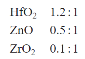
Castellanos Ortega et al.[205] reported resists based on Zr, Hf, and Ti oxo clusters and methyl methacrylate as a major ligand. The clusters were identified as Zr6O4(OH)4(MМА)12, Hf6O4(OH)4(MМА)12(HOBut), and Ti8O8(ММА)16 where MMA is the methacrylate residue (Fig. 9). Resists based on hafnium oxo clusters had the highest sensitivity among the tested materials. Lines with a 50 nm half-pitch were obtained using exposure doses of only 3.5 mJ cm–2 and a radiation source with 13.5 nm wavelength. Nevertheless, the solubility contrast was weak, and none of the lines were resolved at higher doses. Treatment of silicon wafers with hexamethyldisilazane prior to resist deposition improved the solubility contrast and made it possible to achieve smaller critical dimensions (22 nm half-pitch).
![[{"id":"Ys-35RhNZ1","type":"paragraph","data":{"text":"Structure of the Zr<sub>6</sub>O<sub>4</sub>(OH)<sub>4</sub>(MМА)<sub>12</sub> and Hf<sub>6</sub>O<sub>4</sub>(OH)<sub>+</sub>(MМА)<sub>12</sub>(HOBu<sup>t</sup>) oxo clusters.<sup>205</sup> ©SPIE Proceedings, 2019."}}]](/storage/images/resized/roUmOI7Nvtn01GysmphExG6YXTT4BtGFCGSoxigz_xl.webp)
8.2. Resists based on Sn
Tin-containing resists being developed for EUV lithography are hybrid metal-organic compounds based on oxo clusters.
An example of such oxo clusters [(RSn)12O14(OH)6]X2 (Fig. 10) was reported by Cardineau et al.[194][206][207] It was found that on exposure to EUV radiation, the [(BunSn)12O14(OH)6][p-CH3C6H4SO3]2 thin film obtained by spin-coating is converted to compounds with a lower solubility in aqueous isopropyl alcohol. Photolysis of the organic ligand after EUV exposure activates the cluster, which results in agglomeration and formation of a negative tone image. To optimize the lithography characteristics, the authors synthesized oxo clusters with various counter-ions X = [C6H5CH2COO], [OCOCOO], [OCOCH2COO], [HCOO], [C6H5COO], and Cl and organic ligands R = (CH2 = CH – CH2), Bun, Ph. It was found that the sensitivity of the resist decreases with increasing molecular weight of the counter-ion X; however, the quality of lithography and resolution markedly increase. The best line-and-space pattern with a 50 nm half-pitch was formed for X = [C6H5CH2COO]; however, the exposure dose was 690 mJ cm–2. Similarly, the quality of lithography improves for R = Ph; this is also accompanied by a decrease in the sensitivity (510 mJ cm–2). The best lithographic performance (a 18 nm resolution line pattern) was achieved for R = Ph and the inorganic counter-ion X = Cl:. However, even in this case, a relatively large exposure dose was required (350 mJ cm–2). Despite the fact that the sensitivity of these oxo clusters is low, the authors suggest that selection of organic ligands could solve this problem.
![[{"id":"d_LpVo6_YZ","type":"paragraph","data":{"text":"Structure of the oxo clusters [(RSn)<sub>12</sub>O<sub>14</sub>(OH)<sub>6</sub>]X<sub>2</sub> .<sup>207</sup> © SPIE Proceedings, 2017."}}]](/storage/images/resized/I3TiPoQHlJCrLH0nfjvDyOJCwybXcoicgXPvHeMu_xl.webp)
The sensitivity of tin oxo cluster-based resists can be increased not only by chemical modification, but also by selecting the appropriate development method and bake conditions.[207] Experiments involving large area exposure (contrast curve) showed a dependence of the image quality on the initial layer thickness and the post-exposure bake temperature. The 30 nm half-pitch line-and-space pattern formed at an exposure energy of 34 mJ cm–2 is hardly visible, but becomes clearly seen when post-exposure bake is used before developing (100°C, 30 s) (Fig. 11).
![[{"id":"PQzRCBNQjQ","type":"paragraph","data":{"text":"SEM images of the results of lithography of [(RSn)<sub>12</sub>O<sub>14</sub>(OH)<sub>6</sub>]OH<sub>2</sub> without (on the left) and after (on the right) post-exposure bake.<sup>207</sup> © SPIE Proceedings, 2017."}}]](/storage/images/resized/VISaRFgscmDC9YrPHVMCeuUdzXssBepFyWDAZVLz_xl.webp)
Further study of the tin oxo cluster [(BunSn)12O14(OH)6](ОН)2 carried out by Bespalov et al.[208] established that the negative mask formation occurs in several stages. Atomic force microscopy examination of the exposed samples before and after the development shows that the electron beam exposure results in a denser material compared to the original resist, while long-term exposure leads to further densification. This behaviour is consistent with the successive reactions caused by electron irradiation; the authors presented a simplified reaction model A → B → C (Fig. 12) involving the loss of carbon and cross-linking of the inorganic SnOx moieties. Thus, B is an insoluble mixture of units with a low degree of cross-linking, while C reflects the subsequent formation of a denser network. It is noteworthy that electrons with an energy of only 1.2 eV can cause noticeable chemical changes in the resists. In addition, it was calculated that the solubility switching requires less than 10 electrons with an energy of 2 – 38 eV per molecule, which corresponds to an average reaction volume of 0.15 nm3 per electron.
![[{"id":"HUtQevm6l9","type":"paragraph","data":{"text":"Model of successive densification of the material based on [(BunSn)<sub>12</sub>O<sub>14</sub>(OH)<sub>6</sub>]ОН<sub>2</sub> during exposure.<sup>208</sup> © ACS Applied Materials & Interfaces, 2020."}}]](/storage/images/resized/8yfe2ltxO53TLULifYN56yiDeaKSQp7nTG3vMTKR_xl.webp)
According to a study of organotin compounds [(BunSn)12O14(OH)6]2+(O2CCH3–)2 , [BunSn(O)O2CCH3]6 , and BunSn(O2CCH3)2 (Fig. 13) carried out by Sharps et al.,[209] electron beam exposure is accompanied by elimination of butyl groups, which are desorbed from the core surface, followed by elimination of acetate groups in the order depending on the bond strength. However, not all of the ligands are eliminated. The presence of residual ligands on the inorganic core causes their cross-linking. This gives a product that is described most adequately as a metal oxo polymer. The structure of organotin compounds affects their sensitivity to electron beam exposure, but does not influence the structure of the resulting metal oxo polymer (in all cases, the type of the reaction product is the same).
![[{"id":"OvAJC28ipB","type":"paragraph","data":{"text":"Structures of organotin compounds studied by Sharps et al.<sup>209</sup> © Chemistry of Materials, 2019."}}]](/storage/images/resized/JvmkcezFS1nvr1SOIxbjFMGFQIGqgxxb9WtcF4Bc_xl.webp)
The nature of organic ligands primarily influences the spatial structure of the cluster and the cluster packing in the resist film, as was demonstrated for the organotin compounds [R1Sn(O)O2CR2]6, where R1 = Bun; R2 = H, CH3, C4H9 , CH2(C6H5), (CH)(C6H5)2 .[210]Presumably, this should influence the sensitivity to radiation. However, the authors concluded that the stability of the carboxylate radical that is formed upon radiation-induced cleavage of the core periphery makes a greater contribution to the sensitivity than the geometry. Thus, among the clusters considered here, the diphenylacetate cluster with R2 = (CH)(C6H5)2 would require less energy for cleavage, whereas the formate cluster (R2 = H) would require the largest amount of energy. The assumption made by the authors was confirmed by Liu et al.,[211] who studied the organotin compounds of type 63, where R = But, Prn, CH3, H. The compound containing the But group had the highest sensitivity to EUV exposure and showed the highest contrast (Table 16).
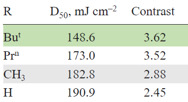
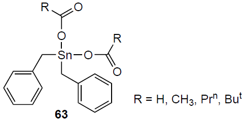
Commercial tin-based Inpria YA Series resists exhibit high resolution and a sensitivity that is relatively high for this type of resist. Exposure using various instruments provides a 13 nm half-pitch resolution (exposure dose of 35 mJ cm–2; ASML NXE:3300B scanner) and an 11 nm half-pitch resolution with roughness of 1.7 nm (EUV interference lithography using equipment of the Paul Scherrer Institute).[25]
The exposure dose tends to increase on going to lower half-pitch values; however, this parameter depends on the equipment used for irradiation.[25] The etch selectivity of Inpria YA Series resists over the spin-on-carbon (SOC) coating* was approximately 40 : 1, which allowed the use of ultrathin (20 nm) films, thus decreasing the probability of appearance of pattern defects such as line collapse.[195]
Ku et al.[212] reported a negative resist based on tin oxo clusters with fluorinated ligands for EUV lithography. The authors assumed that electrons released from Sn atoms upon exposure to EUV radiation diffuse into the outer fluorinated layer of the resist and cleave the C – F bonds to form radical species, which are then bonded to one another to form an insoluble residue. Under EUV lithography conditions, thin films of the resulting fluorinated resist can be used without post-exposure bake, with the resolution of the lithographic image reaching 10 nm.
* Spin-on-carbon (SOC) is a liquid carbon-containing material used as an intermediate layer in multilayer photoresist systems in the manufacture of semiconductors.
8.3. Resists based on Zn
Zinc absorbs light more efficiently than Hf or Zr; therefore, it is considered preferable for producing highly sensitive photoresists for EUV lithography. Zinc-containing resists are hybrid metal-organic compounds based on oxo clusters. The oxo clusters Zn2(BzA)4(AcOH · NEt3)2 and Zn2(m-TA)4(AcOH · NEt3)2 were reported by Xu et al.;[213] the clusters were prepared from zinc acetate dihydrate, triethylamine, ethyl acetate, and benzoic acid (BzA) or meta- toluic acid (m-TA). The Zn2(m-TA)4(AcOH · NEt3)2 resist (Fig. 14a) was used for EUV lithography: a 15 nm half-pitch pattern was formed for exposure dose of 47 mJ cm–2. The authors also obtained images characterized by a smaller half-pitch (14 and 13 nm), but lithographic patterns had numerous defects (Fig. 14b,c). In the future, modification of the oxo cluster by replacement of organic ligands could give materials with specified molecular structure and properties.
![[{"id":"Pp5PfapV8x","type":"paragraph","data":{"text":"(<i>a</i>) Structure of the Zn<sub>2</sub>(<i>m</i>-TA)<sub>4</sub>(AcOH · NEt<sub>3</sub>)<sub>2</sub> oxo cluster; (<i>b, c</i>) SEM images of the results of lithography with (<i>b</i>) 15 nm resolution and (<i>с</i>) 13 nm resolution.<sup>213</sup> © Chemistry of Materials, 2018."}}]](/storage/images/resized/C1UrriClrIMuM9f6L9vJelRTbwdZguft6iEQalT8_xl.webp)
Resists based on zinc nanoparticles with methacrylate ligands were used for DUV lithography at 254 and 248 nm wavelengths.[214]The resulting zinc nanoparticles had a small size of 0.9 – 3 nm and were readily soluble in commonly used media such as PGMEA to be deposited by spin coating. The solution was colourless and transparent up to a concentration of 20 mass %. A resist containing 5 mass % nanoparticles and 5 mass % PAG or an equal amount of a photoradical generator showed the possibility of forming lithographic patterns on exposure to either 254 or 248 nm wavelength. However, the patterning requires relatively high energies of 150 mJ cm–2, and the resolution does not exceed 500 nm.
Another type of oxo clusters was described by Thakur et al.[215-217] These clusters were synthesized from Zn4O(TFA)6 (TFA is trifluoroacetate) and methyl methacrylate (ММА). Identification of the synthesis products revealed the formation of oxo clusters of two structures, Zn(МMA)5 containing five methyl methacrylate residues and Zn(МMA)4(TFA) containing four ММА and one TFA residues (Fig. 15). Although these clusters were unstable and prone to hydrolysis and polymerization (structural changes occur after 2 months of storage of this compound as a crystalline powder and after 4.5 h when the compound is deposited on a substrate), this period of time is sufficient to perform lithographic patterning and subsequent processing. On EUV exposure, the Zn(МMA)4(TFA) cluster made it possible to form a 22 nm half-pitch pattern, with the exposure dose being 12 mJ cm–2 and LWR being 5.7 nm. Lines with a larger half-pitch of 30 nm are characterized by low LWR not exceeding 2.8 nm at comparable exposure doses.
![[{"id":"MsvuLv1-i1","type":"paragraph","data":{"text":"Structure of the Zn(МMA)<sub>4</sub>(TFA) oxo cluster.<sup>215</sup> © SPIE Proceedings, 2019."}}]](/storage/images/resized/hfaysuMSWDtgb9vgSJCgL1lL61yF619Bx0UzrdrO_xl.webp)
8.4. Resists based on Al
Organic aluminium compounds can be used as resists. Grenci et al.[218][219] reported negative resists based on a system containing 80 mass % boehmite nanoparticles [Al2O3/AlO(OH)]. The material was synthesized by the sol – gel method from 3-glycidoxypropyltrimethoxysilane (GPTMS) 64, which contains an epoxide ring that acts as a cross-linking agent. These systems are distinguished by high etch selectivity over silicon (60 : 1). This value was obtained in a series of tests involving deep X-ray lithography and reactive ion etching by an SF6/C4F8/Ar gas mixture. However, the surface quality and LER of the pattern were far from optimal due to the size of the nanoparticles, which was on average 25 nm. This large particle size results in high roughness; usually, the size of nanoparticles and oxo clusters used in resists does not exceed 3 nm.
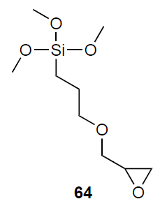
An improved negative resist system produced by the sol – gel method, particularly by the hydrolysis and subsequent condensation of Al(OC2H5)3 and (CH3O)3SiC6H5, showed better lithographic performance.[220] Patterns with a resolution of 200 nm and film thickness of 30 – 40 nm were formed at an exposure dose of 9 J cm–2. The material was developed in concentrated hydrochloric acid. A very high etch selectivity, exceeding 60, was achieved for the silicon etching relative to the mask in reactive ion etching with a fluorine-containing gas plasma.
Grenci et al.[219] described a similar resist obtained also by the sol–gel method from Al(OBus)3 and (CH3O)3SiC6H5 . Using electron beam lithography, isolated lines with a width of 20 nm were produced. The authors suggested that, despite the lower resolution compared to other inorganic resists, this material may be in demand due to its high etch selectivity (more than 60 relative to silicon).
Tiwale et al.[221] reported a new positive organometallic resist based on aluminium nanoparticles obtained by vapour-phase infiltration synthesis. Using atomic layer deposition, Al(CH3)3 was applied onto a PMMA layer deposited on a substrate by spin-coating, and then Al(CH3)3 was treated with vapour to convert it into aluminium oxide (AlOx). The amount of AlOx deposited in the PMMA matrix was controlled by varying the number of cycles. These resists demonstrated a high contrast of 30 for electron beam lithography; a three-dimensional pattern was obtained on silicon with a high aspect ratio (approximately 17), owing to an etch selectivity of approximately 71.2, which is much higher than that of commercial resists such as PMMA, ZEP, and HSQ resists.
8.5. Resists based on other metals
Atoms of other metals can also be used to fabricate resists.
Resists based on In nanoparticles demonstrated good image contrast for micron-scale patterns obtained by exposure to radiation at 248 nm wavelength with an exposure dose of 150 mJ cm–2.[20]
Passarelli et al.[222] reported negative resist systems based on Sb carboxylates with polymerizing olefin substituents (65a – d). A resist based on compound 65b demonstrated an exceptional sensitivity of 5.6 mJ cm–2 in the formation of a lithographic pattern with a resolution of 35 nm. The authors estimated the effect of substituents R1 and R2 in [R1nSb(O2CR2)2] on the lithographic performance. It was found that antimony carboxylate-based resists achieve good sensitivity due to the presence of organic groups containing double bonds that can polymerize on exposure to radiation. A comparison of a number of Ph3Sb(O2CR)2, where the carboxylate O2CR is acrylate, methacrylate, styrenecarboxylate, or acetate, indicated that substituents capable to polymerizing are more sensitive to radiation than non-polymerizing substituents; the resist sensitivity decreases with increasing bulk of organic substituents (Table 17).
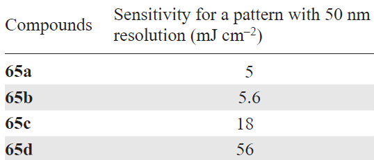
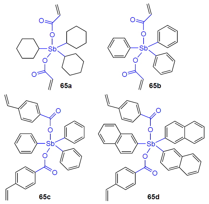
Generally, the contribution of bulky substituents to the increase in the sensitivity exceeds the contribution of the number of unsaturated substituents capable of polymerization.
Sortland et al.[223] investigated the photoreactivity of mononuclear platinum and palladium complexes. Although many platinum and palladium complexes have relatively low sensitivity to EUV radiation, the authors found that L2M(CO3) metal carbonates and L2M(C2O4) metal oxalates (M = Pt, Pd) are sensitive to EUV radiation. Metal carbonates 66a – d form a negative mask while oxalates 67a – d behave as positive tone resists. Studies have shown that palladium-based resists are more sensitive than platinum-based ones. Using the resist based on 67d, lithography images with 30 nm linewidth were produced at an exposure dose of 50 mJ cm–2 and LER = 7.5 nm.
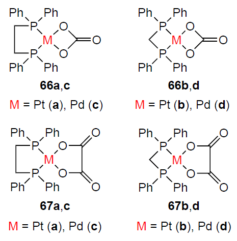
The use of noble metals in the resists considerably increases their cost for industrial applications, which calls into question the expediency of further development in this area from an economic standpoint.
Oxalate complexes of cobalt, iron, and chromium 68 also exhibit sensitivity to EUV radiation, forming negative images,[224] with the resists based on cobalt complex showing the highest sensitivity (Table 18). The resolution limit of the resist based on the cobalt complex was 22 nm with LER of 4 nm and exposure dose of 30 mJ cm–2.
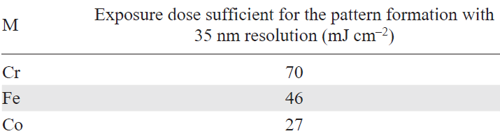
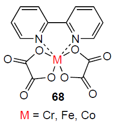
Ghosh et al.[24] described non-chemically amplified polymer resists based on (4-(methacryloyloxy)phenyl)-dimethylsulfonium triflate (48) with ferrocene side units. The proposed resists were prepared by copolymerization of monomers containing EUV-sensitive sulfonium groups. Lithographic images with 18 nm half-pitch and LER = 2.2 were obtained. However, the sensitivity of this resist was relatively low (128 mJ cm–2).
Lewis et al.[225] developed new organometallic negative tone resists based on heterometallic rings containing chromium and nickel atoms. The general structure can be represented by the formula [NH2(CH2 – CH═CH2)2][Cr7NiF8(O2CBut)16]. Preliminary investigation of this compound showed a resolution of 40 nm pitch in the electron beam lithography, but the resist sensitivity was low. To increase the sensitivity, HgCl2 and HgI2 were incorporated into the heterometallic ring. This markedly increased the sensitivity of the resist while maintaining high resolution. The resist [NH2(CH2–CH═CH2)2][Cr7NiF8(O2CBut)15(O2CC5H4N–HgI2)] (Fig. 16) and the chlorine analogue showed the sensitivity not only to electron beam but also to EUV radiation. The addition of mercury iodide to the resist formulation made it possible to achieve a resolution of 15 nm for electron beam lithography and 16 nm for EUV lithography, but even in this case, the exposure dose was 244 mJ cm–2. Low sensitivity is not the only apparent drawback of this approach. The use of mercury compounds on an industrial scale raises many questions related to the environmental and public health issues.
![[{"id":"2LdOVy1sy1","type":"paragraph","data":{"text":"Structure of the cluster"}},{"id":"Js0yVvL53f","type":"paragraph","data":{"text":"[NH<sub>2</sub>(CH<sub>2</sub> – CH═CH<sub>2</sub>)<sub>2</sub>][Cr<sub>7</sub>NiF<sub>8</sub>(O<sub>2</sub>CBu<sup>t</sup>)<sub>15</sub>(O<sub>2</sub>CC<sub>5</sub>H<sub>4</sub>N – HgI<sub>2</sub>)].<sup>225</sup> ©SPIE Proceedings, 2022."}}]](/storage/images/resized/hKHBb9xYNHlqJhUPaZMQcaibZE7bxOq2zFXWB10G_xl.webp)
9. Conclusion
Having considered the trends in the development of resist compositions over the past 20 years, we can identify several important issues.
1. The RLS triangle trade-off has not yet found an ideal solution. Moreover, new metal-based resists that are currently being developed have inherited this problem: while exhibiting excellent resolution and LER performance, they generally lag far behind commercial chemically amplified resists in terms of sensitivity, requiring higher exposure energies. This means that they are not yet ready for industrial-scale production, where everything is governed by cost-efficiency considerations (especially the operation of expensive radiation sources).
2. The international publications show an obvious shift of focus from polymer materials to molecular glasses and metal oxo clusters. Although the market of commercial resists is still dominated by polymer-based compositions, the introduction of new materials is clearly underway. It is quite difficult to track this process, as in the competitive environment, many companies prefer not to disclose key technology details under the pretext of trade secrets. One thing is certain: the implementation of any new scientific idea in industry is generally a slow process, due to established production routine and equipment designs.
In this context, the development of a new lithography technique featuring a new wavelength and new resists could have an unexpected impact on global scientific and industrial trends, sparking a surge of interest in this topic and active research and development in this field.
3. No one has previously developed resists specifically designed to operate at a wavelength of 11.2 nm. A distinctive feature of this wavelength is that it is located immediately beyond the L-edge of silicon absorption (λL = 12.4 nm). However, the global experience in the development of resists for 13.5 nm lithography, as discussed in this review, makes it possible to evaluate and select the most promising approaches to solve this problem. Therefore, we believe that the solution to the problem lies in the most underrated type of resist, that is, silicon-based resists. They can be based on either silsesquioxanes or polymeric compounds containing organosilicon functional groups. As can be seen from the review, silicon-based resists are not the most actively developed area. However, a combination of classical methods for resist manufacturing discussed in this review and the functionalization of silicon-containing moieties may give an impetus to the development of new types of resists sensitive particularly to 11.2 nm wavelength.
In any case, an understanding of the chemical processes that occur in resist materials during exposure, development, and bake has always been the key issue of all studies directed toward the development of new materials. This knowledge will make it possible to produce new resists with enhanced performance, which could bring modern X-ray and EUV lithography to a new level. This, in turn, will inevitably affect the whole microelectronic industry. The question of how quickly this leap in development might occur remains open.
The study was performed within the State Assignment FFUF-2024-0022 and supported by the Russian Science Foundation grant No. 21-72-30029-П.
10. List of abbreviations and symbols
AI — artificial intelligence,
ASML — Advanced Semiconductor Materials Lithography,
BA — butyl acrylate,
BzA — benzoic acid,
CAR — chemically amplified resist,
DBU — 1,8-diazabicycloundec-7-ene,
Dill C — C parameter of Dill’s model,
DUV — deep ultraviolet,
ESCAP — environmentally stable chemical amplification positive,
EUV — extreme ultraviolet,
GC-MS — gas chromatography–mass spectrometry,
GG developer — standard developer used in the LIGA (Lithographie, Galvanoformung, Abformung) process, a mixture of 2-butoxyethoxyethanol, morpholine, 2-aminoethanol, and water,
GPTMS — 3-glycidoxypropyltrimethoxysilane,
4-HS — 4-hydroxystyrene,
HFIBMA — heptafluoroisobutyl methacrylate,
HSQ — hydrogen silsesquioxane (HSiO3/2)8 ,
IPS — isopropyl alcohol,
LER — line edge roughness (nm),
LIGA — Lithographie, Galvanoformung, Abformung, a deep X-ray lithography technique,
LWR — line width roughness (nm),
MA — methacrylate,
MAA — methacrylic acid,
MAN — methacrylonitrile,
MIBK — methyl isobutyl ketone,
ММА — methyl methacrylate,
NILS — normalized image log slope,
OCA — octyl α-cyanoacrylate,
PAG — photoacid generator,
PEB — post-exposure bake,
PGMEA — propylene glycol monomethyl ether acetate,
PHOMS — poly(4-hydroxy-α-methylstyrene),
PHS — poly(4-hydroxystyrene),
PMMA — polymethyl methacrylate,
PSCAR — photosensitized chemically amplified resists,
RET — resolution enhancement techniques,
RLS — resolution/LER/sensitivity,
St — styrene,
m-TA — m-toluic acid,
TFPCA — tetrafluoropropyl α-chloroacrylate,
TFA — trifluoroacetate,
TSMC — Taiwan Semiconductor Manufacturing Company
t-BOC — tert-butoxycarbonyl group.
References