Keywords
Abstract
This review is devoted to an important part of the chemistry of nanomaterials synthesized by laser deposition methods. The structural and composition features of these nanomaterials formed the key trend of research in this field: catalytic and sensing properties. This is not the only application where these materials show promise, but it is undoubtedly the most important one. Until very recently, research in this area was the preserve of specialists in laser physics, electronic and semiconductor technology, and nonlinear optics. The goal of this review is to partially fill the information gap and discuss the role of chemical factors that enable the preparation of nanomaterials with high catalytic and sensing properties. This will enable interested researchers to optimize the laser synthesis processes by deliberately selecting the composition of the starting materials and precursors relying on the information on possible phase compositions and crystallographic characteristics. The discussion of the chemical aspects of laser synthesis is preceded by a brief description of the fundamentals of pulsed laser deposition (PLD) method and laser-induced chemical liquid-phase deposition (LCLD) of metals from solutions. The description is focused on the formation of the phase structure of nanoparticles and nanofilms, which determines their sensing and catalytic properties. The prospects of using laser deposition processes for the design of nanomaterials for hydrogen energy, medicine, organic and inorganic catalysis, and ecology are also analyzed.
The bibliography includes 219 references.
1. Introduction
Laser ablation of a target followed by transfer of the flux of nanoparticles to the substrate (PLD)[1-4] and laser-induced chemical liquid-phase deposition of pure metals from solutions of metal salts or complexes (LCLD)[5][6] attract attention of researchers as facile and effective methods for the manufacture of additive nanomaterials for a broad range of applications in science and technology. The applications include microelectronics, sensor technology, heterogeneous catalysis, and manufacturing of materials possessing high strength or unique electrophysical characteristics. Although the history of both methods, especially PLD, is rich in new ideas, the current state of research has not yet progressed beyond the stage of primary accumulation of information. There is extensive information base on the catalytic, sensing, mechanical, and electrical properties of materials obtained by laser deposition methods. In some cases, local fundamental models have been proposed to describe the mechanisms of formation of nanostructured films, deposits, or nanoparticles under conditions of a particular single experiment. However, these models, like almost the whole field of research, are the responsibility of specialists in laser physics, physical electronics, and nonlinear optics. Meanwhile, there is a gap between the physical model of formation of nano-precipitates and the physicochemical properties of the obtained materials, which can be filled using fundamental knowledge of physical chemistry, solid state chemistry, and laser chemistry. First of all, this applies to the problem of phase composition of the obtained nanostructures, which is, in our opinion, a key issue.
The major role of interfacial interactions in the formation of the sensing and catalytic properties of nanostructures obtained by LCLD was first highlighted in the Refs [5-8]. All other factors are less significant. This applies, in particular to physical factors of the process including laser radiation wavelength, intensity, and pulsed or continuous nature; composition of the gas atmosphere or amount of vacuum; the presence of electromagnetic fields; surface preactivation, the distance between the target and the substrate, etc. In some cases, they affect the phase composition of the target material, generating an aberration of the physicochemical model of the process.
The unique character and the main scientific and technological prospects of the laser deposition methods are associated with the following features.
1. They provide the formation and low-temperature stabilization of crystalline and amorphous phases that exist only at high temperatures when any other methods are used, such as highly supersaturated solid solutions and crystal polymorphs that have not been detected under ambient conditions. Hence, these nano-precipitates possess unique physicochemical properties.
2. In addition, the PLD method makes it possible to form a specified stoichiometry of the nano-precipitate, which reproduces the stoichiometry of the target. The most important feature of PLD is that all PLD processes can occur without a change in the stoichiometry of the deposited layers relative to the ablated ones. The possibility of controlling the composition and properties of PLD nanolayers by controlled variation of the composition of the target is a major advantage of this method over other high-energy techniques. The synthesis is carried out in pulsed mode; therefore, nanoscale quantities of substances can be metered out with a resolution of a few microseconds.[9] This is a unique and very important feature that gives the PLD method considerable advantages over other, nonlaser methods for the generation of nanostructured coatings, such as traditional chemical vapour deposition (CVD).[8]
Somewhat beyond the topic of this review, we would like to note that, apart from the classic laser ablation of a target in a gas or in a vacuum, pulsed laser ablation in liquid (PLAL) is also used. This process also appears promising for the production of nanomaterials owing to the simplicity and accessibility of the process. Today, PLAL is already an environmentally friendly, simple, and inexpensive method for the production of ultrapure carbon nanomaterials (CNMs). Over the past two decades, various CNM allotropes have been obtained using PLAL, including graphene/graphene oxide nanosheets, carbon nanotubes, graphene oxide quantum dots, nanodiamonds, carbogenic nanoparticles, polynuclear crystals, and carbon-encapsulated metal nanoparticles. PLAL is barely used to produce sensing materials. However, certain features of the LCLD method imply that further development of PLAL should be expected.[10]
This review pursues the goal to draw attention to the phase aspect of the laser deposition theory and to stimulate more detailed and thorough research in this area. We have no doubt that the time has come for a more complete integration of the provisions of interfacial interaction theory into the construction of physicochemical models of PLD and LCLD, which will ensure substantial progress in this field.
2. Fundamentals of the pulsed laser deposition method
The pulsed laser deposition method involves the surface destruction of a target in which structural fragments of the substances forming the target are detached and transferred to a remote substrate under the action of high-energy laser pulses.[1-4] The process takes place in a vacuum or in an inert gas atmosphere to prevent high-temperature oxidation. The deposit on the substrate is formed by an additive mechanism. The absorption of laser radiation pulses by the target gives rise to ablation plasma. The laser ablation consists of three stages:[11]
(1) absorption of photons by the surface of the target. The laser beam energy is converted into the energy of excited electronic states, and then into thermal energy. As a consequence, the temperature around the irradiated area rises to several thousand Kelvin, with the heating rate being up to 1011 K per second.
(2) Subsequent evaporation of the target material and formation of bulk plasma. Fragments of the heated surface are knocked out of the target upon multiphoton ionization, thus forming a plume. It also actively absorbs laser radiation, which leads to secondary heating. A shock wave is generated in the atmosphere surrounding the ablation products.[12-14]
(3) Expansion of the beam accompanied by massive emission of atoms, molecules, electrons, ions, clusters, and nanosized particles from the target surface into the surrounding gas or vacuum medium (Fig. 1).
![[{"id":"TcNa83w_mi","type":"paragraph","data":{"text":"Schematic diagram of the PLD production of nanostructured films in a vacuum or gas atmosphere: (<i>1</i>) laser radiation source, (<i>2</i>) high-energy-density beam, (<i>3</i>) focusing system, (<i>4</i>) target (ablated material), (<i>5</i>) ablation plume, (<i>6</i>) flux of target nanofragments, (<i>7</i>) substrate, (<i>8</i>) nanolayer of materal of the target, (<i>9</i>) gas or vacuum chamber."}}]](/storage/images/resized/7L9WZSEEoWTBcvsteFfg16UXGAUux6qI1HixORL3_xl.webp)
If nanoparticles laser-ablated from the target in vacuo are directed to a prepared substrate, they can form nanosized films, single nanoparticles, island structures, or other coatings. A large part of these materials possess unique electrophysical properties. In some cases, effects of superionic transfer are implemented[15-17] and low-temperature stabilized non-equilibrium ordered supramolecular structures are formed.[18-20] These materials are promising for the manufacture of solar energy cells or microsensors.[12][13] Another promising application is the design of nanocatalysts for selective organic synthesis.[21]
The vacuum PLD method was first proposed by Smith and Turner in 1965 for the manufacture of semiconductors and dielectric thin films using a ruby laser, which is still used for the same purpose.[22] To achieve relatively high ablation rates for metal systems (approximately 0.01 nm per pulse), high laser fluences (over 5 J cm–2) are required.[23][24] Under these conditions, a PLD film at the instant of formation also consists of high-energy particles. This creates conditions for high surface mobility of the deposited particles and free diffusion of the particles over the substrate surface. As a result, good adhesion to any substrates used in the versatile PLD technique for thin film deposition is observed mot often.
When the laser fluence is 8 J cm–2, the average kinetic energy of ablated ions is more than 100 eV. The average energy of ablated electrically neutral atoms is much lower (approximately 5 – 10 eV). High-energy particles enable the formation of metastable phases, including nanocrystalline phases, highly supersaturated solid solutions, or amorphous films over a wide range of compositions. For example, in the Fe – Ag eutectic system, in which solid solution regions are virtually absent in the equilibrium state, the single-phase Fe(Ag) region can be supersaturated to a much higher extent than in the case of traditional precipitation methods, namely, the Ag content may be 39 to 57 at.% at room temperature.[25]
As mentioned above, this is a very important and underestimated feature of laser methods for the formation of solid phases. Modern science does not yet offer other methods for stabilization of crystalline and amorphous phases with this high degree of non-equilibrium under ambient conditions.
One more unique feature of PLD is as follows. The effects of formation of a supersaturated solid solution as the base of uniform films are responsible for implantation of the highest-energy ions from the overall flux on the substrate, mixing of these ions with the already deposited material, and film growth in the layers below the surface layer (so-called subsurface growth mode).[26] The implantation of high-energy species at high laser fluences exceeding 6 J cm–2 into the molecular layers located below the film surface generates additional structural defects. This may account, in particular, for high mechanical stress measuring tens of GPa. This effect was described by Krebs et al.[27] and can be detected by the shift of powder X-ray reflections toward smaller scattering angles.
Numerous theoretical works devoted to the PLD method do not claim, most often, the status of a unified theory relating the physical conditions of deposition (laser wavelength, intensity, and operating mode; composition and pressure of the gas atmosphere (amount of vacuum); substrate temperature and the target–substrate distance) to the structure and properties of nano-precipitates and the outcome of deposition. Quantitative estimates of the influence of physical parameters are made specifically for each particular process and material and do not aim to provide a common fundamental generalization for the method as a whole. This appears to be due to the fact that, as has already been noted, the physical and chemical properties of nanomaterials are mainly determined by their phase and stoichiometric compositions, and data of this type are available in enormous quantity. There is no direct, unified functional relationship between these data and the deposition parameters. This relationship is unique for each particular system.
Study of the effects of various physical parameters of the process on the outcome of deposition yields a heterogeneous, unsystematic picture. This is due to the multiplicity of research objects (targets and substrates), high diversity of applied lasers, and heterogeneity of goals and applications. It is hardly possible to cover the whole picture within not only a single review, but also within a monograph. Therefore, we will address the most recent and significant publications devoted to phase composition and structure of nano-precipitates.
The influence of laser wavelength on the morphology, structure, and optical properties of PLD films of nanostructured lithium niobate (LiNbO3) used in optoelectronics was described by Salim et al.[28] and Son et al.[29] Lithium niobate is an important optoacoustic materials widely used in nonlinear optical devices, including waveguides. A LiNbO3 film was formed on a quartz substrate under pulsed laser radiation at wavelengths of 1064 and 532 nm. It was shown that the wavelength influences the electrical and optical parameters of nanolayers, including their thickness and crystallographic characteristics. The transition from lower-energy to higher-energy radiation (from 1064 to 532 nm) is accompanied by a decrease in the spectral transmittance, absorbance, and the band gap of the deposited nanomaterial, but the reflectance and refractive index of the film increase. Meanwhile, X-ray diffraction measurements show that the crystal structure of LiNbO3 becomes less amorphous and more ordered; the size of film microcrystals also increases. The thin film of LiNbO3 prepared at a substrate temperature of 570 K gives best results for the manufacture of optical waiveguides.
Most often, researchers have one or two lasers with different wavelengths at their disposal; hence, no systematic studies of the spectral dependences of the phase composition and structure of PLD films are available from the literature; the data are limited to comparison of the results of deposition at one or two wavelengths.
Some studies are devoted to the role of the target–substrate distance. Vakulov et al.[30] investigated the effect of the target–substrate distance during the pulsed laser deposition on the composition and electrical properties of LiNbO3 thin films. The LiNbO3 thin films prepared at a target – substrate distance of 120 mm were depleted in niobium (0.7 at.%) compared to the films obtained at a target–substrate distance of 20 mm (11.0 at.%). As the target – substrate distance changed from 20 to 120 mm, the charge carrier mobility increased from 24 to 395 cm2 V–1 s–1, while the concentration of charge carriers decreased from 3 × 10¹³ to 1 × 1012 cm–3.
Other methods for the control of the properties of nanolayers such as the change in the laser radiation parameters and the substrate composition were illustrated in relation to the growth of graphene films.[31] Graphene films are used for the synthesis of materials with p – n junctions for electronic and optoelectronic applications and for the design of sensors using electrochemical methods. Quite a few parameters including the heating and cooling rates, power of the laser, the growth time, and the substrate temperature and composition influence the microstructure and morphology of graphene films. This review lists data from several dozens of publications without systematization. Each of the dozens of researchers cited used their own set of deposition parameters starting with the type of laser, which ranged from argon lasers (l = 193 nm) with a pulse duration τ = 20 – 30 ns to neodymium Nd : YAG laser (neodymium yttrium aluminium garnet, λ = 1064 nm, τ = 6 ns). The pressure in the vacuum chamber varied from 1.3 × 10⁻⁴ to 1 × 10⁻⁴ Pa. The substrate temperature varied from 570 to 1470 K, the target – substrate distance was 35 to 50 mm, and various types of pyrolytic graphite carbon served as the target. This scattered set of initial data cannot be used to develop a unified theoretical model. The accumulation of primary technical data has not yet reached the stage of theoretical comprehension.
Apart from physical factors, factors that can be classified as chemical were also analyzed in the study. The phase composition of graphene films was varied by depositing them onto layers of catalytically active metals such as nickel, copper, and tin. In particular, the sequence of deposition of nickel nanolayers was varied: either a nickel layer on top of a carbon layer on a substrate or, conversely, a carbon later on top of a nickel layer. It was shown that the order of layers considerably affects the quality of graphene films. This changes their morphology and crystal and supramolecular structures. The overall conclusion from the results of the study is clear: no single parameter is responsible for the formation of high-quality graphene over a large area; all growth conditions must be optimized to achieve a better graphene quality compared to that grown using chemical vapour deposition (CVD) or mechanical polishing of the surface of a monolithic material. The key advantage of the produced group of electrodes was a stable electrochemical response over a period of 22 days. Owing to the multilayer structure of the sensitive layer, the number of implanted molecules of the target analyte was higher than that on other commonly used substrates such as glassy carbon or boron-doped diamond. The work opens up good prospects for the development of self-assembling 3D graphene electrodes with various sensing functions and can be applied to fragile sensing objects such as biomolecules or living systems.
Basak and Das[32] reported the PLD production of graphene films using epitaxial processes on substrates made of various metals such as Ni, Cu, Co, and Fe, which had lattice parameters of 0.352, 0.361, 0.251, and 0.287 nm, respectively. Among them, Ni and Cu had the least lattice mismatch with graphene (0.357 nm). Depending on the parameters of the lattice contact layer and the solubility of carbon, supramolecular layered, columnar, or dendritic structures were formed on metal substrates (Fig. 2).
![[{"id":"2c7DYIc-uU","type":"paragraph","data":{"text":"Schematic image of the main types of supramolecular structures formed on substrates upon laser deposition processes: (<i>1</i>) layered, (<i>2</i>) columnar, and (<i>3</i>) dendritic; (<i>4</i>) substrate orientations relative to the structures shown in the Figure. The green dotted line shows the conditional phase boundaries."}}]](/storage/images/resized/dOXDtD8hwlA1w12lMg4W2GUdQ2JZxhkIZS2R067H_xl.webp)
The authors assumed that the epitaxially oriented structure of the deposit could potentially lead to the design of materials with unique strength characteristics.
While attempting to develop a theoretical base for the PLD process, Lysne et al.[33] designed a theoretical model that described distribution of the material over the substrate after a single laser pulse hits the target. The mathematical modelling and simulation of the process were implemented in the PyPLD open Python library. The model is applicable to the description of deposition of both single-component thin films and multicomponent, but compositionally uniform films on Cr- and Ni-doped silicon wafers 50.8 mm in diameter. In other words, the model still does not touch upon the phase composition problem, considering a priori that the deposited material is a single phase. The model was experimentally tested for only one laser–target–substrate system; therefore, the model versatility was not yet verified. The experiment was carried out for Cr- and Ni-doped silicon films using variable-angle spectroscopic ellipsometry for highly precise determination of optical properties and the thickness of calibration films. The PyPLD algorithm was used to design films with a specified thickness variation. Considering the calculated film thickness and distribution function of the material deposited on the substrate per laser pulse, the thickness variation D(x,y) for single-component films was approximated using the expression
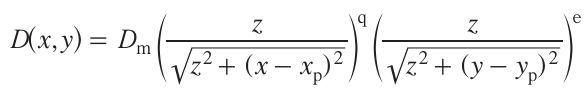
Here Dm is the maximum film thickness, z is the distance between the target and the substrate, xp and yp are coordinates of the centre of the plume relative to the substrate centre (x = y = 0, for T = T0), and q and e are empirical approximation parameters describing the rate of change of the thickness of the standard calibration sample.
The intensity of the laser beam hitting the target was approximated using the Lambert – Beer law in interpretation (2):
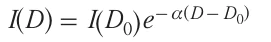
Here I(D) is the reduced laser beam intensity in an ablated layer of thickness D under the target surface, I(D0) is the intensity before the laser beam hits the target, and α is the coefficient of radiation absorption for material of the target. The optical penetration depth δ (attenuation length) is found from equation (3):

The radiation absorption coefficient of the material α is related to the refractive index n by equation (4):
Here λ = 2πc/ω is the laser radiation wavelength, c is the velocity of light, ω is the angular velocity, nk0 is the absorption index, k0 is the attenuation index. Equations (3) and (4) indicate that the beam penetration depth into the target δ is directly proportional to the reciprocal of laser radiation energy and inversely proportional to the refractive index n of the material.
The ablated material is transferred to the substrate. The film formation and growth on the substrate surface is simulated by the standard crystallization model, including the nucleation and crystal growth stages.[34] The nucleation precedes the formation of nanocrystals with the smallest size. The nucleation is caused by fluctuation-induced local nanosecond concentration supersaturations of melt microvolumes with atoms of one of the components. This is followed by the formation of nanocrystal (Fig. 3a) or degradation of the nucleus (Fig. 3b) depending on whether the nucleus has lost or gained one atom of the crystallizing component immediately after the nucleation.
![[{"id":"McSoGolFE6","type":"paragraph","data":{"text":"Diagram of the nucleation and crystallization stages of nano-precipitates: (<i>a</i>) conversion of the nucleus to the nanocrystal and (<i>b</i>) degradation of the nucleus."}}]](/storage/images/resized/Sh9jjHX2fnr24KApgCMS5aod4TAy4j6zdmTvlvR3_xl.webp)
According to this model, the nucleation and crystal growth on the substrate surface results in the conversion of species and ions from the plasma (jet) phase to the crystalline (solid) phase. According to the model, the emergence and growth of a thin crystalline film depend on the following parameters: laser radiation energy, pulse repetition rate, density and degree of ionization of the ablated material, substrate temperature and physicochemical properties, and inert gas pressure (in the case of gas atmosphere). Among these characteristics, the most important thermodynamic parameters that determine the growth mechanism include the substrate temperature Ts and the relative local concentration supersaturations Cs arising by the fluctuation mechanism in the solid phase of the material under the action of plasma during the deposition. These two parameters are interrelated by equation (5):
Here kB is the Boltzmann constant, R is the rate of deposition, and Re is the equilibrium deposition rate at temperature Ts. Equation (5) shows that the concentration supersaturation of the substrate with a component directly depends on the substrate temperature. A low supersaturation is characterized by a high rate of nucleation of numerous isolated centres of crystallization, giving rise to isolated clusters on the material on the substrate surface. As the number of clusters being formed on the substrate surface increases, the cluster density grows, while the size of separate nuclei, on the contrary, decreases to the atomic level. An increase in the supersaturation due to a high substrate temperature leads to enlargement of structural fragments via coalescence (which, in some cases, resembles the formation of liquid drops). The minimum thickness D at which the thin film being formed becomes continuous is defined by equation (6):
where T is the substrate temperature, R is the rate of deposition, A is the constant depending on the properties of the material.[35]
This model describes the simplest case of PLD process for one particular system, but further model development and extension to more complex cases provides possibility of further development of the method, which may reduce the labour intensity of preliminary experiments.
The proposed mathematical model neglects one more important factor of formation of PLD films, namely, the composition and pressure of the gas atmosphere in the ablation chamber (when inert gases are used). Sturm et al.[36][37] showed that the factor of plasma jet dispersion on gas atmosphere molecules can be significant.
When pulsed laser deposition is carried out in an ultrahigh vacuum, the deposited material consists of a high proportion of ions with kinetic energy around 100 eV. These species cause additional composition fluctuations on the film surface (they induce local supersaturation and nucleation). It was shown that high-energy fluctuations can be suppressed by using inert gas atmosphere in the chamber. The authors studied the effect of Ar gas medium on the pulsed laser deposition of metal systems (Ag, Fe, Fe/Ag).[36] The time-of-flight data for plasma particles and film formation rate were measured, which indicated a decrease in the average energy of plasma particles with increasing Ar pressure and also a decrease in the resputtering and local supersaturation at the plasma – substrate interface. The pressure Pr at which the film growth due to the plasma sputtering considerably decreases is approximately 4 Pa. This effect is attributable to scattering of a dense plasma cloud of ablated material in dilute inert gas.
Under argon atmosphere at a pressure much below 10 Pa, the decrease in the average particle energy is due to scattering of the dense cloud of the ablated material moving through dilute gas.[38] On the way to the substrate, some of the high-energy ions are scattered away from the target–substrate trajectory, whereas slower atoms hit the substrate surface without any obstacles. At higher gas pressures, the expansion of the plasma plume gives rise to a second shock front between the plasma plume and the surrounding gas, which hinders the expansion of the plasma and causes mechanical stress in the deposited film. This, in turn, affects the texture of the film (fibrous, island, etc.). The decrease in the kinetic energy of particles is accompanied by diminution of mixing and structural redistribution effects[24][39][40] and switching of the residual mechanical stress in films from compressive to tensile. Thus, parameters of the gas atmosphere can ba used to control the film texture. This is possible if the kinetic energy of the deposited particles is below the atomic displacement threshold energy (approximately 25 eV for most metals). Under these conditions, the subsurface implantation of particles into the growing film is minimized, but the particles still have enough energy for structural deformations and fluctuations on the film surface due to high surface mobility. Under these conditions, alternation of the composition of the target or variation of other physical parameters of deposition makes it possible to obtain multilayer structures that would be non-equilibrium under ambient conditions and would have clear-cut phase interfaces, as was shown for the Fe/Ag system.[36] As emphasized above, exactly this factor has the crucial effect on many physical, catalytic, and sensing properties of deposited films.
The theory of the effect of phase inhomogeneities on the sensing and catalytic properties of laser-induced deposits was formulated in detail in relation to laser-induced chemical liquid-phase deposition (LCLD) and is discussed in the next Section. Here, it is worth mentioning that the main statements of the theory are fully applicable to PLD films.
The modern literature devoted to PLD is highly extensive;[31][41-45] therefore, in this review, the primary attention is given to most recent publications. They reflect the current trend of switching from improving the PLD technique to the search for new applications, first of all in the field of sensors and catalysts, and in some other fields.
3. Fundamentals of laser-induced chemical liquid-phase deposition method
The fundamental principles as applied to the LCLD method have been already addressed in detail in our previous reviews;[5][6] therefore, here we give a brief account concerning only the main issues, sometimes disputable, of the description of LCLD mechanism.
While speaking about the mechanism of the laser-induced chemical liquid-phase deposition, we have in mind not a particular single chemical reaction or physical process, but a unified set of conjugate chemical reactions and processes occurring at the focus of a laser beam in a solution and on a dielectric substrate.
Laser-induced chemical liquid-phase deposition is based on the chemical reduction of a metal taking place in a local volume of a solution at the focus of a laser beam and results in metal deposition on the surface of the dielectric substrate (Fig. 4).
![[{"id":"VsSnUOzFRe","type":"paragraph","data":{"text":"Diagram of LCLD process. (<i>1</i>) laser radiation source; (<i>2</i>) high energy density beam; (<i>3</i>) focusing system; (<i>4, 5</i>) solution of salts and/or organic metal complexes that are reduced at the focus of a laser beam; (<i>6, 7</i>) substrate acting simultaneously as the ablation target."}}]](/storage/images/resized/O5ikKfSTaQC8VDxibY1yc5UyK6QUgX9SWTmOI3Ew_xl.webp)
The liquid used for laser deposition is an aqueous solution containing a transition metal salt, pH regulating agent (the reaction takes place in an alkaline medium), and an organic ligand that is coordinated to the transition metal atom via OH– groups (usually, this is a salt of tartaric acid, EDTA or Trilon B, or polyhydric alcohol). Most often, the ligand acts simultaneously as a reducing agent in the metal deposition reaction. In the first LCLD experiments, a separate reducing agent (formaldehyde) was added. In the most general form, metal reduction in a laser radiation field is described as
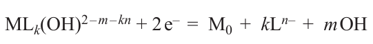
Here M is metal; L is ligand; and k, m, n are stoichiometric coefficients. In some cases, nanoparticles of the metal being reduced (e.g., copper) serve as catalysts for reduction proceeding, in particular, beyond the laser radiation field, i.e., this reaction is autocatalytic.[5][6]
If we imagine that, instead of the dilute gas or vacuum medium inherent in PLD, the laser-ablated substrate particle enters a liquid medium, then the plasma plume will be extinguished in close proximity to the target. A liquid medium, which is viscous (compared to the gas), precludes the deposition of the target nanofragments on the substrate, even when it is located in the close vicinity to the target; their energy is rapidly quenched by the hydration shell, the plasma metal ions are converted to hydrated salts, bases, or complexes, aqueous-organic catalytic reactions take place on hot and cold nanoparticles.[46] The PLD mechanism is transformed into af PLAL – LCLD superposition.
Pulsed laser ablation in liquids (PLAL) is accompanied by hydrodynamic sputtering[47] followed by scattering of nanoparticles and ions from the surface of metal targets to the bulk solution.[48-50] The magnitude of mechanical stress arising in the target may exceed the dynamic tensile strength of the material, leading to its cavitation.
The subsequent fate of nanoparticles may vary. When no special measures are taken, they often coagulate in aqueous solution to give relatively large aggregates[51][52] and thus lose their specific properties. In some cases, this process is deliberately stimulated to remove nanoparticles.[53-56] The spontaneous coagulation limits the use of PLAL methods.
Thus, it is necessary to emphasize the difference between PLAL and LCLD. In the former case, the substrate (also acting as the target) is ablated, and the plasma plume is directed to the solution where the products of ablation are scattered and can subsequently undergo spontaneous growth and coagulation. Conversely, in the latter method, nanoparticles are precipitated from a solution and are densely deposited on the substrate. The additive LCLD technology forms nanoparticles on a substrate by a nucleation mechanism followed by spontaneous coalescence, which continues for some time after the laser radiation has left the deposition zone.[57][58] In other words, the difference between the two techniques consists in the method used to prepare the precursor, that is, metal nanoparticles.
The most recent publications[59] suggest that the ablation in a liquid, unlike that in a gas atmosphere, may give rise to not only electrically neutral metal nanoparticles, but also hydrated ions. These ions participate in electrochemical reactions involving the substrate material in a zone remote from the laser beam focus. If organic ligands with a high complexing capacity are present in the solution, these ions can be involved in the secondary laser deposition.[59] This is reflected in the fact that LCLD is always accompanied by laser ablation of the substrate, but the total deposit + substrate weight changes very slowly during the reaction.
The fundamentals of the LCLD method were developed by Kordás et al.[60] and Shafeev.[61-63] This method causes a lot of debate, because there is no common opinion on the relationship between the thermal and photochemical components of deposition and no clear understanding of the mechanism of deposition on the substrates that are transparent at most laser wavelengths in the visible and near-IR regions, which applies to substrates made of quartz glass and ST-50-1 sitall (crystalline glass ceramics). The intense heating of the transparent substrate in the laser focal spot is considered by many researchers to be inexplicable, despite the facts that the existence of this phenomenon cannot be denied and that causes for the phenomenon have already been explained in the literature.[64-66]
The point is that the fluctuation absorption of one photon at a frequency ν of, for example, 5.6 × 10¹⁴ Hz by an m-atomic group of the substrate may substantially increase the energy of this group. The fluctuation can be caused, for example, by a photon hitting a crystal lattice or surface defect, in particular, in the interfacial region (if it exists in the substrate). The energy increment can be correlated with a temperature rise of the atomic group by ΔT. According to Bal’makov and Muradova[66]
When ν = 5.6 × 10¹⁴ Hz, one has ΔT ~ 9 × 10³ m–1. In other words, for small molecules (m ~ 10), ΔT ~ 103. Certainly, the number of such high-energy atomic groups is relatively small. However, it is these groups that participate in the first elementary events of laser-induced deposition. As the first reduced metal atoms appear on the substrate, the absorption coefficient at these points sharply increases, the group becomes non-transparent at the focus of the laser beam, and intense local heating begins. The average number (mathematical expectation) of photons N–absorbed over time Δt (s) in a group of m atoms is given by
Here αm (cm–1) is the absorption coefficient; J (W cm–2) is the laser fluence, and ν (Hz) is the photon mode frequency. Since the temperature changes DT ~ N̅/m, with all other factors being the same, then
According to equation (10), an increase in the optical absorption coefficient α by several orders of magnitude leads to a pronounced increase in the local temperature.[67] The mechanism of formation of the first clusters markedly depends on the nature and number of active sites per unit area of the substrate surface (k). The relative geometry of these sites is also important. When the number of deposited metal atoms exceeds a certain critical value mc, an autocatalytic deposition process is activated, and the deposition rate substantially increases. The fraction U of these rapidly growing groups containing at least mc atoms by instant t amounts to
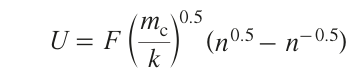
Here
m̅ is equal to the average number of metal atoms located on one active site over time t. The above model corresponds to two main deposition mechanisms at low and high metal concentrations described by Shafeev;[68] they are similar to PLD processes.[33] When the mc /k ratio is relatively low (~ 10), the autocatalytic mechanism determines the metal deposition for 0.1% of the sites (U = 0.001). On average, only 0.4 n of the total number of metal atoms are deposited at the sites. Hence, 0.1% of the active sites ‘absorb’ other inactive sites. The other limiting case correspobds to the mc/k ratio being much greater than 10. Then the autocatalytic mechanism determines the metal deposition simultaneously at all of the sites (for mc/k > 105, n > 0.99). The metal deposition occurs in one stage. The metal is deposited directly from the solution onto the substrate upon thermally or photo induced redox reaction in solution at the dielectric boundary.[69] Intense heating of the local reaction area initiates a series of processes. The first one is the change in the substrate properties in the heated area (including surface activation) and also chemical reactions (decomposition, reduction, or oxidation of reactants, etc.) at the substrate/liquid interface.[5][68] Due to the high rate of metal reduction at the laser beam focus, fast spontaneous diffusion of the reducing agent from the solution area to the area of laser beam focus takes place. This process may continue until the metal cations in the solution are exhausted.
Laser-induced chemical liquid-phase deposition can be classified as an additive method, as it involves metal deposition directly in the area of formation of metal tracks at the laser beam focus and in the adjacent area. The possibility of positioning the laser beam with a micrometre accuracy allows the manufacture of conductors with a small cross-sectional area and a small distance between parallel metal tracks. This does not require the manufacture and use of high-precision and expensive templates, which are needed in most traditional metal deposition methods. A laser beam ‘draws’ an intricate track under the action of a simple mechanical scanner. This feature is one of the main advantages of LCLD over traditional precision metal deposition methods.
Using other known laser metal deposition techniques (the above-mentioned CVD,[8] electrochemical deposition, chemical deposition from solutions assisted by ultraviolet radiation, laser induced forward transfer deposition,[70-73] etc.), it is possible to fabricate conductive structures on metals, dielectrics, and semiconductors. However, extensive application of these methods is limited by the need to use expensive precise templates and by difficulties associated with the production of films with a specified crystallographic structure and controlled stoichiometry. There are also problems related to the high toxicity and low volatility of many organometallic compounds. In the laser-induced forward transfer (LIFT) deposition, laser radiation serves for cleavage of metal-organic and organosilicon framework polymers (e.g., copolymer of copper(I) hexafluoroacetylacetonate and trimethylvinylsilane) and subsequent metal deposition onto a substrate.[70] The polymer evaporation starts at a temperature of 290 – 320 K (0.5 – 130 Pa), while degradation begins at 370 – 420 K.
The width of tracks deposited using the LCVD method is several tens of micrometres at a deposition rate of several to hundreds of micrometres per second,[74][75] which is insufficient for some practical applications. The use of most gas-phase, chemical, and electrochemical methods[76-79] requires special equipment (templates) to deposit a layer of solid metal-containing compound on a substrate and to subsequently remove the non-decomposed film or excess deposited material. Therefore, PLAL and LCLD methods, which do not require the above operations, appear to be most accessible for mass implementation. They are least costly in terms of equipment and can be easily implemented using a standard laser scanner.
The outcome of the LCLD process depends on three main groups of factors.
1. Physical factors: laser radiation power; laser scanning speed of the substrate; temperature of the environment and the solution. Strange as it may seem, these are the least influential factors; this was discovered many years later when chemists joined the research in this field.
2. The most significant factors are chemical factors including the composition of the solution, component concentrations, and pH. These parameters are selected empirically for each synthesis, as they can act in different directions and have non-monotonic effects. For example, an increase in metal concentration can accelerate or, conversely, inhibit the deposition. The same is true for pH effect.[80]
3. Properties of the substrate surface: structure; the presence of activated and catalytic sites; defective structure; phase composition; and chemical properties of dielectric components. The influence of these factors is very large and is partially described by Kochemirovsky et al.[81]
The deposits produced by LCLD are formed more actively on surfaces with grain boundaries and interfaces.[81] Comparison of the results of deposition of copper structures on three different dielectric surfaces, that is, quartz glass, polycrystalline alumina, and glass ceramics (sitall) reveals the following trends.
(1) The deposition is somewhat more efficient on glassy material than on alumina, which correlates with the views on the glass being a disordered crystal, i.e., this surface is markedly more defective than the surface of a crystal, but high conductivity and adhesion still cannot be achieved. Seo et al [82] improved the quality of deposition on a glassy surface by preliminary etching.
(2) The replacement of alumina and glassy silica by ST-50.1 glass ceramic material, which is a composite based on the same components (60.5% SiO2; 13.5% Al2O3; 8.5% CaO; 7.5% MgO; and 10% TiO2), that is, a microcomposite of rutile (α-TiO2) and cordierite (2 MgO · 2 Al2O3 · 5 SiO2), results in a considerable increase in the rate of deposition. Presumably, the best result obtained on the surface of glass ceramics is due to the presence of several phases in the substrate, which has a beneficial effect on the surface activation and further laser-induced deposition of copper from the solution. This process is a few orders of magnitude more intense (Fig. 5). This assumption can be substantiated by the following considerations.
![[{"id":"vGtYzbggvq","type":"paragraph","data":{"text":"Schematic image of the morphology of LCLD products on various types of surfaces (<i>1 – 3</i>) and the corresponding photomicrographs (<i>4 – 6</i>): copper (<i>1, 4</i>) on a single-phase crystalline Al<sub>2</sub>O<sub>3</sub> surface, (<i>2, 5</i>) on a single-phase amorphous (glassy) SiO<sub>2</sub> surface, (<i>3, 6</i>) heterophase ST 50.1 glass crystalline surface. Photographs from the authors’ archive."}}]](/storage/images/resized/Gmn5hiwfDamsc6Q1Mp79Cmf6shGdnzUVakzJ4PHk_xl.webp)
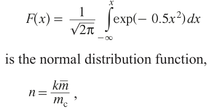
The way in which the nucleation mechanism for the formation of the first LCLD clusters considerably depends on the nature and number of active sites (k) per unit area of the substrate surface has been described above. Apart from the number, the relative geometry of these sites is also important. In the case of a heterophase substrate, the k value is proportional to the length L of all interfaces over an area of 1 cm2. The interface length l for a particular nanofragment is given by

Here V is the degree of dispersion. The number of these nanofragments in 1 cm² area is proportional to Uv2/3V 2, where Uv is their volume fraction. Taking account of equation (6) gives the following expression for the length L of all interfaces in 1 cm2 area:
The probability of the elemental step of formation of a k-atomic cluster per unit surface area and per unit time ρk can be found as follows:
The coefficient b empirically takes into account the properties of interfaces, the composition of the solution, the intensity of laser radiation, the speed of movement of the focal spot, and some other parameters.
The interfaces usually form an electrical double layer. An increase in the concentration of metal cations near negatively charged regions leads to numerous correlation effects. For our purposes, it is important that the k value increases. Thus, there is a complete analogy with the mechanism of PLD described by Ogugua et al.,[35] i.e., the low-concentration mechanism produces a surface with a high degree of coverage with small crystallization centres, while the high-concentration mechanism produces a surface with a low degree of coverage with large crystallization centres.[33][34][68] A decrease in the density of crystallization centres with increasing metal concentration has also been predicted.[83][84] The presented calculation is in good agreement with experimental data reported in the literature.[33][34][68]
The difference between the structures deposited on the substrate by LCLD observed with increasing distance from the focal spot centre (the highest energy density),[6][85][86] indicates that the structure of the deposits is affected by the thermal conditions of deposition. At the initial time instant, deposition occurs uniformly and synchronously in the form of concentric areas corresponding to a particular thermal zone. In practice, this is manifested as appearance of an axial channel in the vast majority of deposited structures, irrespective of the type of substrate or composition of the solution. The axial channel is present both in the deposit track and in the substrate material (Fig. 6).
![[{"id":"uwUrcUra4_","type":"paragraph","data":{"text":"(<i>a</i>) Profile of a deposited structure: (<i>1</i>) substrate (target), (<i>2</i>) laser beam; (<i>3 – 5</i>) thermal zones of deposition: (<i>3</i>) high-temper ature zone, (<i>4</i>) medium-temperature zone, and (<i>5</i>) low-temperature zone, (<i>6</i>) deposited LCLD track. (<i>b</i>) Electron micrograph of a cross section of a molybdenum track formed on an ST-50.1 glass ceramic substrate. (<i>c</i>) Electron micrograph of the surface of the same track (sorbitol as the reducing agent and the ligand, pH = 8). Copyrights for Figs 6 <i>b,c</i> belong to Elsevier.<sup>7</sup>"}}]](/storage/images/resized/bhymfJff17zD3luq6iEaRiIvuFwqCTk4WAqXCFeU_xl.webp)
This indicates that LCLD always competes and coexists with PLAL laser ablation in liquids. The ablated material of the deposit or metal substrate is partially converted back into a source of ions for LCLD.[59] The cycle continues until the ion source is completely depleted.
Three temperature zones differing in the mechanisms of metal deposition can be conditionally distinguished (see Fig. 6): (3) focal (high-temperature) zone located in the region of focused laser beam (5 – 7 μm in diameter) or in the close vicinity of the beam focus. The focal spot zone is characterized by high temperatures, 1300 to 2800 K and more, according to various estimates.[87][88] This is a zone of possible formation of metal deposits by mechanisms described in the literature,[89][90] i.e., similarly to processes occurring in metallurgy. The highest-energy atomic groups are located near the focus of the laser beam. The proportion of these groups decreases as the distance r from the focus increases. The temperature T(r), which characterizes the average energy of the groups that initiate the autocatalytic laser-induced deposition also decreases. The linear dependence of the width of LCLD track on the laser radiation power W imposes a number of limitations on the analytical relation for the deposition rate R at the point with the coordinates X, Y.
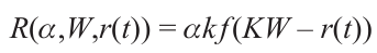
Here, it is taken that
When W satisfies the inequality,
After appropriate mathematical transformations, considering that R ~ exp(–U/T ), where U is the activation energy, the relative temperature T(r(t)) at time instant t for the point with the coordinates X, Y is given by
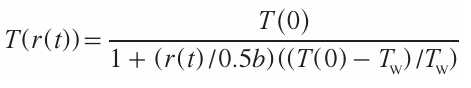
Here Tс = T(0) is the temperature at the laser spot focus, Tw = T(0.5b) is the temperature at the track boundary. The temperature fields formed by a variable-power laser on the surface of a dielectric substrate for various radiation powers can be represented as a family of curves r = f (W).[87][88]
At this point, we come to the key issue of the review. All possible types of dielectric substrates can be divided into single-phase and heterophase (composite) substrates. In general terms, the task of initiating the formation of a crystalline metal deposit on a dielectric surface is reduced to the generation of a sufficient number of active sites for crystallization per unit surface area of the dielectric. The most important point in this process is the appearance of an activated site on a dielectric substrate. Laser radiation is a potent stimulating factor for this activation.[5][6] Metal deposition on single-phase surfaces under ambient conditions is impossible without laser irradiation, since unirradiated areas do not contain a sufficient number of activated sites.
The activated sites, that is, Schottky and Frenkel defects well known from the literature[91] and all kinds of dislocations and surface atoms can be conditionally divided into two types: (1) point or (2) linear defects of a semiconductor or dielectric surface. Their main feature is that they are sensitive to thermal conditions and the material prehistory. They can appear and disappear as a result of heating.[92] A single-phase homogeneous material usually contains an insufficient number of these sites for the formation of a monolithic film or track even after laser activation, since laser exposure may have opposite consequences. Therefore, deposits formed by LCLD on single-phase materials have island intermittent structure and low stability. The focal spot of the laser is likely to both generate new activated sites and destroy existing ones formed via natural chemical processes and thus decrease the activation capacity of the dielectric surface. The single activated sites remaining in the laser temperature zone do not always accelerate the deposition, since their concentration is comparable with the concentration of similar sites on the initial surface.
The attempts made by A.G.Shafeev[61-63] to carry out preactivation of single-phase surfaces by mechanical methods (polishing, scribing) and chemical etching resulted in increase in the specific surface area of the material, but did not affect the concentration of active sites. In other words, the number of active sites increased in proportion to the effective area of the substrate, but not due to a change in the nature of the material.
Phase interfaces have an important advantage over point and linear defects of a single-phase dielectric surface: heterophase surfaces tend to have much more defects concentrated at interfaces; furthermore, these defects cannot disappear under the action of high temperatures (annealing) and exist up to the liquidus temperature of the two-phase system. The formation of metal clusters and deposits in the laser radiation field may continue to proceed on multiphase dielectrics even in the temperature range between the solidus and liquidus lines. In the interfacial regions, either all sites needed for deposition, similar to those formed upon the Shafeev activation,[61-63] are present initially, or the laser irradiation of the interface in the high-temperature or medium-temperature zone in solution induces the conversion of interfaces into zones with increased concentration of the predeposited metal clusters. These predeposits can act as active sites in the low-temperature zone even after the surface has left the laser irradiation area and thus promote further metal deposition by electrochemical mechanisms.[61-63][68]
The appearance of effective charge regions is attributable to laser-induced bending of energy bands of the dielectric and formation of activated sites as metal atoms or other defects that promote charge transfer.[68]
The reduction of metal ions on laser-activated surface sites occurs at temperature T1, which exceeds some threshold value. In addition, active sites of different nature are characterized by different T1 values.
The sites formed by interfaces can be active at temperature T2, which is lower than T1. The temperature T2 corresponds to overcoming of the energy threshold for electron transfer resulting in the metal ion reduction. It is reasonable to assume that the electron work function of the negatively charged phase decreases upon the formation of a phase boundary (Fig. 7).
![[{"id":"lfbSJebiox","type":"paragraph","data":{"text":"Diagram of defect formation on a non-activated single phase surface (<i>a</i>) and activated heterophase surface (<i>b</i>)."}}]](/storage/images/resized/rzY3KARVzpVIxIWfbJavWSZ8fiEo2wjugAIq2IRQ_xl.webp)
Therefore, the activation of defects associated with phase heterogeneity starts at lower temperatures, with the surface area of their activation having a greater length along the r axis (FIg. 8). The lower the temperature dependences, the higher the derivatives dr/dw, with these dependences being nearly linear.
![[{"id":"cl6sWD6U35","type":"paragraph","data":{"text":"Isotherms <i>r = f (W).</i>"}}]](/storage/images/resized/H6UgSzxYFvRIS8mwuzW1bsizt7yjEk5lMAr0t2BU_xl.webp)
The slopes of the plot of the metal (oxide) track width vs. laser radiation power can be used as quantitative characteristics of the substrate in terms of its ability to form high-quality deposits under the action of focused laser radiation. An approximate estimation [90] [93] shows that the temperature near the focusing point of the laser beam for a glass ceramic substrate exceeds 1500 K even at a radiation power of 1.1 W.
In the medium-temperature zone (zone 4 in Fig. 6), the temperature decreases from the focal spot temperature to ≈1300 – 600 K. This corresponds to the temperature range for thermal degradation of organic salts and copper complexes and the formation of copper deposits by other mechanisms, in particular, via chemical reduction of copper compounds [94][95] or reduction of metal oxides and salts by analogy with processes taking place in geological systems.[96][97]
The low-temperature zone (400 K and lower; zone 5 in Fig. 6) is the region of existence of non-boiling aqueous solutions. It can be assumed that this zone on the substrate could have been partially activated earlier during a short period of time spent in the high-temperature zone.[93][98] In the low-temperature zone, coalescence mechanisms are implemented;[99][100] in this case, the predeposited metal acts as a catalytic surface; therefore, in some cases, the reaction follows the autocatalytic mechanism.[101]
Depending on the structure and composition of the substrate, the concentration of metal salt or complex in the solution, the laser power, and the scanning speed, the width of the metal track can range from 10 to 200 μm. The electrical conductivity of the track can vary over a wide range from values close to those of pure monolithic metals to hundreds of kΩ cm–1. The concentration dependence of conductivity parameters is non-monotonic passing through a maximum. The same is true for the variation of pH (Fig. 9).[102] Similar trends were found for copper and are also observed for nickel.
![[{"id":"MESV62johe","type":"paragraph","data":{"text":"Conductivity of copper deposits obtained by LCLD <i>vs</i>. concentration of the copper salt in solution (<i>a</i>) and pH (<i>b</i>).<sup>102</sup>"}}]](/storage/images/resized/09HYJcwNBfb3qcRgc1gInBIEipJbCuzLbLzlcc2V_xl.webp)
Evidently, the pH and concentration values affect the structure of metal complexes in the solution; therefore, the morphology of metal deposits formed by LCLD is determined by the speciation of complexes, which is, in turn, determined by the solution composition and pH (Fig. 10).[80][102][103]
![[{"id":"iq8J7H2SqO","type":"paragraph","data":{"text":"Structures of monometallic and bimetallic mono- and binuclear tartrate complexes in an alkaline solution for LCLD used for the deposition of single-phase tracks (upper row) and heterophase tracks (lower row)."}}]](/storage/images/resized/I5g7W1w82c1gXEMiWUBv8DcgAPQ4cwCXF3qGfHt6_xl.webp)
These complexes possess the following features:
— the ligand is coordinated to the metal through the hydroxyl group;
— if the solution contains ions of two transition metals, the minor metal (present in a lower concentration) is coordinated to the outer sphere of the ligand.
The highest sensing and catalytic activity is inherent in deposits produced from complexes comprising two metals that form an eutectic mixture in the binary phase diagram. Comparison of the data on the effect of metal chlorides added to solutions of copper salts (as a rule, also chlorides) on the properties of copper deposits formed by LCLD with binary phase diagrams of metal systems [103-107] shows that the enhanced electrochemical and sensing characteristics of the copper – cobalt deposits are due to the fact that the Cu – Co system has a peritectic phase diagram, that is, for figurative points located in the liquidus line at equilibrium, one liquid phase is in equilibrium with two solid phases. The presence of two phases results in an abrupt increase in the specific surface area of the deposit, an increase in the total length of the interfaces, and, as a result, an increase in the current or potential response of the deposit in solution.
As can be seen from Fig. 9, the LCLD process occurs in an alkaline medium. The ligand usually performs a dual function: it keeps the metal ion in solution, thus preventing the hydroxide precipitation and also acts as a reducing agent. The most effective reducing agents for the metal during LCLD are compounds with low redox potentials containing OH groups, such as polyhydric alcohols.[86][108] Other functional groups do not produce conductive deposits.[100]
The morphology of deposits obtained by LCLD is affected by surfactants. This occurs through the mechanism of reductive gas formation in the solution, which defocuses the laser beam. It was shown[109] that the addition of non-ionic surfactant actually decreases the adverse influence of the gas formation during the laser-induced chemical liquid-phase deposition of copper. It was found for the first time that the topology and quality of deposited structures are improved as the hydrophilic/lipophilic balance of the non-ionic surfactant decreases, and the produced copper structures have low specific resistance compared to the deposits obtained from solutions without the addition of surfactants.
The electrophysical characteristics of materials obtained by LCLD are directly related to their sensing properties, which are discussed in a separate Section.
4. Heterophase nature of the increased sensing and catalytic activity of materials obtained by laser deposition methods
Similarly to the fact that the highest activity in PLD and LCLD formation of nanoprecipitates is characteristic of heterophase surfaces, the highest sensing activity is inherent in films, tracks, and other deposits consisting of several phases. The nature of this high sensing and catalytic activity is caused by the the charge carrier concentration and mobility difference between two contacting components at the interface. As two solid phases come in contact, the charge carriers are transported across the interface toward the region with a lower concentration and mobility, resulting in the formation of a potential difference, that is, a barrier layer that prevents the charge transfer and ensures the electrical neutrality of the phase regions. In this case, it is often more convenient to perform the charge transfer via common contact with a third phase, which can be represented by a liquid or gaseous reaction medium or a specimen to be analyzed (Fig. 11).
![[{"id":"encdz-2W_e","type":"paragraph","data":{"text":"Diagram of direct charge transfer across the boundary between two contacting solid phases and facilitated charge transfer through reaction or analyte mixtures. Е<sub>1</sub> and Е<sub>2</sub> are average energies of charge carriers in the contacting phases <i>1</i> and <i>2</i>; <i>3</i> is the reaction medium containing objects of catalysis or analytes <i>4</i>, ΔЕ<sub>1</sub> > ΔЕ<sub>2</sub> ."}}]](/storage/images/resized/7NYvk674eDg9GHkLhmI2WrCz2yLzIDX1p6p4HVLw_xl.webp)
The quantity of charge transported across the interface serves as an analytical signal for the sensor or characterizes the activity of the catalyst.
The region of interfacial contact is also characterized by the highest structural disorder in the adjacent layers.[110] Depending on epitaxial characteristics of the contacting phases, the degree of disorder can markedly vary. In some cases, the interfacial layers become amorphous, while in some other cases, they form stable nanolayers of crystalline phases that could not existent under normal conditions or that, in principle, have never been detected in this system before. New electrophysical and chemical processes that are not characteristic of any of the contacting phases existing separately may appear in the disordered region. In the case where these processes affect the charge transfer in some way, we obtain a new sensing or catalytically active material. This applies not only to electron transfer processes, but also to ion transfer in solids.
Solid crystalline, amorphous, or composite substances with electrical conductivity comparable to that of semiconductors, in which charge transfer is entirely or partially performed by ions, are called solid electrolytes. The classic views on ion migration in a solid crystal are associated with the possibility of formation and migration of Schottky and Frenkel lattice defects.[111][112] A regular or irregular disorder in the structure of a solid is a necessary condition for the emergence of ionic conductivity.[110] Various types of amorphization serve as a modern, actively developing method for the generation of structural disorder in monolithic samples and films. This increases the ionic conductivity by a few orders of magnitude.[113-115] The best results along this line were achieved by the PLD method.[116-120] Using this method, it is possible not only to transfer the stoichiometry of the target to the substrate, but also to preserve its structural and chemical characteristics in the deposited layer. In addition, in some cases, PLD solves a very complex engineering problem, since it allows high-quality amorphous deposition of glasses that are prone to crystallization and are, hence, unsuitable for glass-blowing.
For example, sensitive layers of amorphous glass target were deposited[121] by PLD using a COMPex Pro 110 excimer laser with a wavelength of 248 nm (KrF), the maximum pulse energy of 400 mJ, pulse repetition rate of up to 100 Hz, pulse duration of 20 ns, and a flux density of 5.3 J cm–2. This procedure was used to fabricate glass pH electrodes and reference electrodes based on glasses containing gold and TixOy oxides with an exceptionally stable potential and low temperature drift.[121]
Multilayer films consisting of two or more materials differing in the crystallographic structure can be easily produced using PLD. By controlling the number of pulses directed toward the target, it is possible to achieve precise control of the film layer thickness. The high speed of ablation from the target ensures congruent evaporation of the target components and preservation of the stoichiometry during film formation on the substrate. Using PLD, nanolayer films consisting of AgI and chalcogenide glass layers with a total thickness of 1 μm were produced.[122-124] The thickness of alternating chalcogenide glass and AgI layers ranged from 10 to 15 nm (Fig. 12).[16][122]
![[{"id":"AmyZRtXR3r","type":"paragraph","data":{"text":"Photomicrograph and schematic image of a multilayer PLD nanofilm chip in chalcogenide glass.<sup>122 </sup>Copyright Springer."}}]](/storage/images/resized/SianXFyKjNKS2tChJbB5CFc82auO9eyQkEGuNcu9_xl.webp)
The nanolayered PLD material exhibited unique electrophysical, structural, and chemical properties. In the 410 – 430 K temperature range, superionic transition, that is, a sharp increase in the conductivity associated with the phase transition in the AgI sublattice, took place in the material.[123-125] The mobility of ions in the superionic solid state is comparable to, and sometimes even exceeds, the mobility of ions in liquids. As a result, the composite solid electrolyte had a uniquely high specific conductivity of 0.3 S cm–1, with the activation energy for the conduction being 0.07 eV. An increase in the phase transition temperature with increasing layer thickness was observed and reached saturation when the layer thickness was approximately 50 nm. In other words, PLD ensured a unique size effect. In addition, it was found that, apart from the X-ray diffraction reflections corresponding to α-AgI, reflections of a previously unknown phase (X-phase) appeared on heating and were preserved at room temperature. The X-phase appeard when the material was heated (at a temperature below the softening point of glass), together with α-AgI, and had a face-centred cubic lattice (NaCl structure). The lattice constant was 5.81 – 5.82 Å; this corresponds to the high-pressure AgI phase, which occurs in equilibrium state only at pressures above 1.5 GPa.[126]
The chalcogenide platform Ge28Sb12Se60 is actively used for the fabrication of ion selective electrodes, which have been incorporated in multi-sensor systems of the ‘electronic tongue’ type.[127][128] The production of the Ge28Sb12Se60 – AgI heterophase nanolayered ion-selective membrane with enhanced ion response was aimed at increasing the sensitivity of the sensor by an order of magnitude.
The major technological trend of recent years in the PLD fabrication of new sensing and catalytically active materials is to form nanolayered heterophase structures. The PLD compositions are fabricated using alternating metal–semiconductor,[129-131] ionic semiconductor – electronic semiconductor,[132-134] and metal – metal[135] layers. These systems include chalcogenide[135][136] and oxygen glasses,[137-139] metal oxides,[140-142] and pure metals.[143-145]
The LCLD process is less studied than PLD. Among other factors, this is due to the fact that the first works in this field appeared 30 years later.[68][70] Since LCLD is performed in a liquid medium and, with rare exceptions, does not require high-precision templates, this process was initially considered as an alternative to template technologies for manufacturing printed circuit boards. The geometry, morphology, and electrical conductivity of metal tracks were the main structural and electrophysical parameters that have long been the focus of attention of researchers.[5][6] However, in recent years, this idea was rejected because of low rate of the process (within a few millimetres per hour) and high electrical conductivity of the deposits. Currently, this method is used almost completely for the design of heterophase micro- and nanocomposites for sensors.[146] Heterophase microcomposites produced by LCLD are widely employed to design a new family of non-enzymatic biosensors.[77] In addition, the first studies making use of the catalytic properties of LCLD nanoparticles in organic reactions have been reported.[147-149]
5. Sensing properties of PLD and LCLD nanostructures in the gas atmosphere
5.1. PLD sensors
The sensing and catalytic activity of elements and compounds is achieved through similar mechanisms for a wide range of methods used to prepare the sensitive layer. However, nanosensors produced using PLD and LCLD methods have advantages over traditional sensors. This is manifested in faster response and low energy consumption during operation and regeneration. In some cases, it is possible to achieve also better sensitivity, accuracy, and signal stability parameters by forming heterophase layers. The main approach used to achieve this result is to modify the composition of the target or deposition solution using traditional precursors that proved to be effective in other techniques.
Cyza et al.[150] studied the catalytic and sensing properties of the perovskite type oxides (described, for example, by Kaur and Singh[151]). They were obtained by the PLD method. The perovskite oxides with the general formula A2+B4+(X2−)3 are being actively studied due to their simultaneous ionic and electronic conductivity. Perovskites have a great potential for various applications such as gas sensors, automotive exhaust catalysts, methane reformers producing synthesis gas, and cathodes in solid oxide fuel cells. The perovskite LaFeO3 has very good catalytic and sensing properties in the presence of acetone (CH3COCH3), ethanol (C2H5OH), and liquefied petroleum gas vapours and gases such as hydrogen sulfide (H2S), hydrogen (H2), and NO2. Thin films of LaFeO3 are typical p-type semiconductors. The mechanism of gas sensitivity for semiconductor materials is based on changes in the surface electrical resistance on contact with gases. The action of air on the La1 – xSrxFeO3 sensors leads to chemical absorption of oxygen. This results in the formation of a thin space charge layer, which reduces the potential barrier for reactions of reducing gases. The catalytic reduction of surface oxides with organic gases leads to an increase in the space charge layer, which increases the electrical conductivity and the current from an external source. The obtained thin films had a columnar structure[150] and a thickness in the 150 – 170 nm range. A sort of piezoelectric effect was observed: low-symmetry crystal polymorphs demonstrated variability of physical properties, in particular charge carrier concentrations and mobilities, depending on orientation. The difference in the orientation was manifested in the structure of the upper sensitive layer. It had a shape of pyramidal columns, with their tips pointing upward, in the case of LaFeO3 and a plane-parallel shape for La0.9Sr0.1FeO3. The best results were found for pyramid-shaped structures. They showed the highest analytical response: the conductivity ratio at a working temperature of 576 K between the layer that adsorbed acetone vapour and the regenerated layer was 3.75 for pyramidal structures vs. 1.77 for plane-parallel structures. The measured time of response to the presence of 4 ppm of acetone at T = 576 K was 54 s for pyramidal LaFeO3 and the regeneration time was 66 s; the same values for La0.9Sr0.1FeO3 were 180 and 258 s, respectively. In other words, an effect similar to the interfacial contact effect was observed, due to increase in the specific surface area of the material and a change in the morphology. It remains to be added that the PLD synthesis of the sensitive layer for the sensor was carried out without a change in the stoichiometry of the initial precursor (target), which is also important for practical applications.
Another classic material with versatile applications is zinc oxide ZnO. It is used in a pure state as a material for semiconductor and electronic technology, a dye, a catalyst, and as a semiconductor doped with other metals and composites containing other oxides. This is due to low cost and a broad scope of applicability of zinc oxide.[152] In 2008, the amended European Union Restriction of Hazardous Substances (RoHS) directive prohibited the use of lead, cadmium, and mercury.[153] Thus, a pressing need for components containing no lead appeared in Europe. This is why, a lot of studies addressing PLD-ZnO appeared in recent years. In this regard, Fasquelle et al.[154] investigateded the effect of the microstructures of ZnO thin films on the limit of detection (LOD) of hydrogen sulfide (H2S). Zinc oxide thin films were deposited by PLD onto silicon substrates under various conditions to achieve variations in the microstructure. The PLD sensors were compared with the existing commercial semiconductor sensors for H2S gas manufactured by Figaro and Winsen. Good sensitivity values measured at T = 670 K and 100 ppm of H2S and a response time of only 30 s were considered to be promising for the design of commercial sensors.
A heterophase sensor based on PLD-ZnO was reported by Alyamani et al.[120] The authors studied the electrical properties of Al-doped nanostructured three-phase Al – ZnO/p-Si/Al diode. The diode photoresponse served as an analytical signal. Aluminium-doped ZnO films (Al – ZnO) were applied on a silicon substrate by the PLD technique. The structural properties of the films were investigated using transmission electron microscopy and X-ray diffraction. According to X-ray diffraction patterns, light-sensitive films are polycrystalline materials with a hexagonal wurtzite structure, predominantly oriented in the (002) direction. The electrical photoresponse of the diode was analyzed over a wide range of frequencies and light intensities. Using impedance spectroscopy to measure the capacitive and real conductivity components, the authors showed the presence of interface states, that is, lengthy phase interfaces. Comparison with an analogue prepared by the sol – gel method showed the advantage of using a PLD diode as a photodiode or photocapacitor in optoelectronic applications: the intensity and speed of the photoresponse increased.
Sensors sensitive to H2 play an important role in hydrogen energy for the control of hydrogen production.[155] Thin films of n-type ZnO were produced by the new two-target two-pulsed laser deposition technique. This is a new PLD technique in which the laser beam alternatively focuses on two targets. The operating mode of the specially designed laser is adjusted in such a way that every second pulse vaporizes the material from the surface that has been preheated by the first pulse. The first laser pulse vaporizes the material of the target to form a plasma. The second pulse forms a shock wave that accelerates the movement of particles formed by the first pulse toward the substrate. A filter is installed in the path of the ablated flux to block the movement of plasma nanofragments and transmit only atoms. This gives rise to a droplet-free PLD film (Fig. 13).
![[{"id":"cUtRfROi8E","type":"paragraph","data":{"text":"Schematic diagram of the two-target two-pulsed laser deposition: (<i>1</i>) source of two-pulsed laser radiation; (<i>2</i>) variably focused beam; (<i>3</i>) focusing system; (<i>4</i>) flux of nanofragments from two targets; (<i>5, 6</i>) targets for alternating focusing; (<i>7</i>) substrate; (<i>8</i>) nanolayers of target materials; (<i>9</i>) gas or vacuum chamber; (<i>10</i>) filter for the separation of plasma nanofragments."}}]](/storage/images/resized/N0QTXSZTgWGMFCDsmLS4KY7hkXngYbfKtgVgPrjX_xl.webp)
The heterophase nature of the sensitive layer is due to the introduction of dopants into the targets. The dopants (Al, Au) and the type of substrate (Si, SiO2 , glass) were varied during the experiments.[155] The sensing properties of the films were tested by exposing them to an H2 flow in air at operating temperatures ranging from 420 to 480 K. Undoped ZnO thin films deposited on SiO2 substrates at 470 K in an O2 atmosphere at 20 Pa with a laser fluence of 9.6 J cm–3 exhibited the highest sensitivity, detecting less than 3 vol.% hydrogen in air with the response time of less than 3 min at a working temperature of 440 K. A decrease in the working temperature to 420 K was achieved by sensitization of the films after deposition of Au nanoclusters on the surface of the same ZnO thin films.
The PLD method was used to deposit ZnO thin films at room temperature[156] using an Nd : YAG laser with a wavelength of 1064 nm and pulse frequency and duration of 10 Hz and 5 ns, respectively. The incident laser radiation energy varied from 1.07 to 7.13 J cm–2. Gas sensing properties of thin films were evaluated in relation to hydrogen. Thin films were deposited on an Al2O3 substrate (7 × 7 mm²). The mathematical formula for the response had the form:
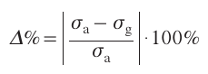
where σa is the resistance of the sensor before gas exposure, and σg is the sensor resistance after gas saturation. The maximum and minimum response for deposition of the ZnO thin film using PLD were achieved for laser fluences of 3.12 and 7.13 J cm–2, respectively. The presence of reducing H2 gas near the surface of the ZnO thin film facilitates the electron transfer between H2 molecules in the atmosphere and oxygen ions adsorbed on the sensor surface, which leads to population of the conduction band by electrons of the acceptor (O2). As a result, the concentration of charge carriers increases and the electrical resistance of the sensor thin film decreases. The conductivity increases with increase in the grain size of thin films caused by a decrease in the number of defective states and an increase in the contribution of grain boundaries. The increase in the grain size of ZnO thin films enhances sensor characteristics. The ZnO crystallinity is also important for the sensitivity of the sensor. As a result, the optimal gas sensitivity was achieved at a laser fluence of 3.12 J cm–2. When the linear dimensions of the nanocrystal edge exceeded 20 nm, the sensitivity increased with increasing grain size.
It should be mentioned that, in addition to formation of heterophase structures, laser methods provide another traditional opportunity for considerable enhancement of the analytical signal: the fabrication of films, nanofragments, and tracks with extensive surface area. Most often, the analytical signal of the sensor is proportional to the specific surface area of the sensing component. Using PLD and LCLD techniques, this value can be increased, in some cases, by several orders of magnitude.[157][158]
An integrated method for improving the sensing characteristics of ZnO was proposed by Dey.[159] Highly porous, pure, silver-doped 3D ZnO nanostructures for the use in sensor systems were formed by PLD. The response of ZnO and Ag – ZnO sensing elements to NH3, CO, ethanol, and acetone was studied under UV irradiation. The presence of Ag nanoparticles in the ZnO nanostructure gave rise to phase inhomogeneities and substantially improved the response of the sensing elements to all of the tested gases. In addition, the authors investigated the effect of simultaneous exposure to UV radiation and to red light on the response intensity of sensing elements and on response and recovery times. It was found that UV irradiation and optimized red irradiation improved the response of the Ag – ZnO sensor to CO, while simultaneously suppressing the response to NH3, ethanol, and acetone. The nanocomposite sensor demonstrated a strong and stable response when exposed to 1 ppm of CO, suggesting the possibility of measuring even lower concentrations.
Apart from ZnO, other metal oxides such as SnO2, TiO2, In2O2, etc. are often used for all sorts of gas sensors.[159][160]
Dhand et al.[160] reported the design of highly porous ZnO, TiO2, SnO2, and MoO2 metallic nanostructures to be used as gas sensors. The samples were obtained by PLD in air at atmospheric pressure. The sensitivity and response time, as well as the regeneration temperature of the sensing elements, were determined for exposure to NH3, CO, acetone, and ethanol. The sensitivity was enhanced by the fabrication of a nanocomposite sensor consisting of a metal oxide (ZnO) and a noble metal (Au nanoparticles). Metal oxide targets were ablated using an Nd : YAG nanosecond laser (Lotis LS-2147). The structures deposited on the substrate by PLD were highly porous and consisted of aggregated nanoparticles with randomly distributed nanofragments. All metal oxide nanostructures showed the highest response to NH3 vapour, with the TiO2-based sensor being most sensitive among them. The response time to ammonia markedly varied among different metal oxide sensors. At a concentration of 10 ppm, it ranged from 12 to 15 s for a TiO2-based sensor and was more than 30 s for an SnO2-based sensor. Sensors based on MoO3 and SnO2 demonstrated the best selectivity to ammonia. The highest sensitivity to acetone and CO was found for the ZnO-based sensor, while the Au – ZnO-based sample showed high sensitivity on exposure to ethanol. It should be emphasized that all results were obtained at room temperature, which demonstrates the promise of this method.
There are also numerous similar studies dealing with graphene.[161-163] Here, the design principle of the gas-sensitive layer was based on doping the graphene surface with noble metals (Pd, Au, and Ag) or on the fabrication of ultrathin oxide (CuO – MnO2 , In2O3 , or Sc2O3) or sulfide (SnS) coatings. This approach provides the formation of sensitive elements for semiquantitative determination (30 ppm) of NO2 and O3.
5.2. LCLD sensors
The LCLD sensors have been addressed in a much smaller number of studies. It was shown that the highly extensive surface of LCLD microsensors is directly responsible for their high sensitivity, short response time, and low regeneration temperature.[164] The highest sensitivity was observed for the detection of low concentrations (≤ 50 ppm) of hydrogen sulfide at temperatures of 570 – 620 K, whereas at temperatures of 570 K and below, microstructures obtained by molybdenum deposition using LCLD are applicable for the detection of ammonia.[7] The highly extensive sensing surface is formed because of the fact that in alkaline aqueous solutions used for deposition, molybdenum exists as anionic species [hydrated molybdate (MoO)32− and paramolybdate (MoO)42− ions], which results in simultaneous deposition of both the pure metal and semiconducting oxides. Molybdenum can have various oxidation states in oxides, which gives rise to defective structures, phase separation, and appearance of numerous active sites. The reaction initiation threshold does not change and remains at ~ 600 mW for pH from 6 to 9. The track width increases from 50 – 100 to 200 – 250 μm as the laser power increases from 600 to 2000 mW in the same pH range. The observed conductivity properties indicate that the tracks obtained from solutions with pH = 6, 7, and 9 are non-conductive. For microstructures produced at pH ~ 8, the measured electrical resistance is more than 0.3 kΩ for a continuous track with a length of 10 mm and a width of 100 μm. The intensity of the response of the synthesized microsensor to various gases and vapours: ammonia (NH3); ethanol, propanol, and acetic acid; and hydrogen sulfide (H2S) in the atmosphere at various concentrations and temperatures is represented as a 3D diagram (Fig. 14)[7] in the concentration – temperature – response coordinates according to relation (17). The three-dimensional approach was used for the first time; this makes it possible to visualize the selectivity areas of the sensor and choose the desired temperature and concentration range for each particular analyte.
![[{"id":"VuSHVSpt8b","type":"paragraph","data":{"text":"Intensity of the response of the Mo – Mo<sub>x</sub> LCLD microsensor to various gases and vapours: ammonia (NH<sub>3</sub>); ethanol vapour (C<sub>2</sub>H<sub>5</sub>OH); and hydrogen sulfide (H<sub>2</sub>S) in the atmosphere at various concentrations and temperatures projected onto the coordinate planes of the 3D function.<sup>7</sup> The symbols on the vertical axis have been changed in accordance with the logic of the notation in this review."}}]](/storage/images/resized/tHphmu1yqOEScqAJnyFbn7cfGIpkpfBgwlze3baC_xl.webp)
The sensor demonstrates good service characteristics: fast response and low regeneration temperature, as can be seen from the comparison given in Table 1.[7][165-172]
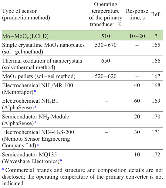
The limited statistics of application of LCLD sensors in gas analysis is attributable to the fact that LCLD has not yet been well developed due to the short history.
6. Sensing properties of PLD and LCLD nanostructures in liquids
Metal, oxide, sulfide, nitride, and carbide nanoparticles, carbon-based materials, and nanocomposites with controlled structural and morphological properties are very promising for numerous sensor applications. Methods based on pulsed laser deposition have a number of advantages over other synthesis methods: simple equipment, the possibility of controlling film structure and composition, adjustable growth rate, and the possibility of stoichiometric transfer in plasma.
Today, a highly relevant problem of sensorics is the development of non-enzymatic microbiosensors for medical and biological applications. Currently, biomedical sensorics is being rapidly developed on the basis of the PLD method. Velumani et al.[173] described prototypes of electrochemical sensor systems prepared by PLD to monitor biomarkers and small molecular targets in common biological fluids, e.g., in blood and sweat; this quickly provides important information about the health status and performance of the human body. The concentrations of certain metabolites, ions, and proteins in saliva, tears, and urine can be monitored on a real time basis using non-invasive, wearable, portable sensors. A part of the review by Velumani et al.[173] is devoted to the identification of numerous biomarkers contained in sweat. In addition to human sweat biomarkers, xenobiotics formed under the influence of environmental factors can also be deposited on the skin and subsequently be dissolved in sweat. Since human skin provides a broad platform for sweat collection and analysis, sensors mounted on the skin can also be used for chemical stimulation of sweat glands and fast collection of the necessary sweat samples in vivo for patients administered with drugs such as pilocarpine, methacholine, and acetylcholine. The main requirements for these sensors include sensitivity, selectivity as well as the convenience of wearing and portability. The physiological monitoring is not limited to analysis of metabolites. The development of portable PLD sensors for measuring high blood pressure was also reported.[174]
Certain difficulties associated with the production and use of enzymatic biosensors for determination of glucose and hydrogen peroxide (components of human blood) have stimulated researchers in this field to seek alternative solutions. The number of recent publications devoted to the development of non-enzymatic sensors based on metal and metal oxide nano- and microstructures is fairly great, which attests to the relevance of the problem. Gougis et al.[175] were the first to describe a non-enzymatic cyclic and pulse voltammetric method for determination of glucose using gold nanostructures deposited by laser pulses on carbon nanotube electrodes. The authors considered a few possible methods of synthesis to achieve different morphology of Au film. It was found that an Au PLD film deposited in a vacuum by 10 000 laser pulses possesses a high specific active surface area with a roughness coefficient of 13.2. In addition, this electrode is characterized by a markedly lower potential for glucose oxidation (–0.28 V) than the traditional Ag/AgCl electrode (–0.6 V). A linear square-wave voltammetric response for the oxidation of glucose was observed up to a glucose concentration of 50 mM with a sensitivity of 25 μA cm−2 mM−1 and a detection limit of 0.1 mM. It can be expected that PLD will soon become the main tool for manufacturing miniature sensors based on microcrystals.
Silver-based materials also have good prospects for the use in oxygen reduction reaction (ORR) and for hydrogen peroxide (H2O2) detection.[176] The importance of monitoring H2O2 is due to the fact that it is a strategic raw material in industry, a disinfectant, and a physiological marker of diseases when present in human blood. The development of an non-enzymatic sensor for H2O2 is of high research interest. Porous silver nanostructures obtained by PLD have attracted interest as primary transducer of the hydrogen peroxide signal owing to their great specific surface area and high electrochemical activity. Using PLD under controlled background gas pressure, Zhao et al.[176] obtained nanoporous Ag structures consisting of nano-sized particles. Structurally similar nanoporous deposits are formed by the LCLD technique (Fig. 15).
![[{"id":"NU5_G3DfvQ","type":"paragraph","data":{"text":"Characteristic appearance of silver nanodeposits obtained by PLD and LCLD methods. Their porosity and highly extensive surface are due to the large number of intergrain voids (photo from the authors’ archive)."}}]](/storage/images/resized/jPn3TXZERTQfIuAox29bOmELa8SxSrBWNxYl8I6x_xl.webp)
Porous PLD-Ag showed good performance in ORR reactions, in particular high selectivity in the detection of H2O2 in the presence of glucose, uric acid, and ethanol. The sensitivity of the sensors varies from 415.0 to –613.1 μA cm−2 mM−1, which is markedly higher than that of a common smooth silver foil (8.1 μA cm−2 mM−1). It is also important that porous PLD-Ag can be deposited on flexible substrates for potential use under challenging conditions.
Thin films of indium selenide (In2Se3) obtained using PLD technique were tested[177] at various gas pressures and at various stages of film formation with the goal of detecting uric acid by cyclic voltammetry (CV), differential pulse voltammetry (DPV), and chronoamperometry. The high sensitivity (0.38 mA mM–1), selectivity, and signal stability of the non-enzymatic biosensor fabricated in this way indicate good sensor activity of In2Se3 .
The application of the PLD method is not limited to the possibility of designing non-enzymatic sensors. This method is also used to improve traditional enzymatic sensors. The LW-SAW commercial enzymatic sensor fabricated using PLD technique,[178] for which the only information disclosed was that it was based on acetylcholinesterase (AChE), was immobilized on three gold substrates with different surface morphologies. The analytical response of this sensor to chloroform was studied. It was shown that the sensitivity and the detection limit are considerably improved when porous layers are used instead of traditional monolithic gold layers. The response to variation of the chloroform concentration for three PLD sensors with different sensitive layer morphology was characterized by much higher frequency shifts than that of the sensors based on monolithic Au layer. The response of all three sensors was linear in the tested concentration range, with no signs of signal saturation.
There are also other recent studies dealing with the development of enzyme-based PLD sensors. Ciriello and Guerriei[179] proposed a new electrochemical method for determining the phospholipase activity based on the use of the biosensor fabricated by immobilization of cholinesterase on the surface formed by oxidative polymerization of pyrrole in the presence of excess oxygen and deposited on a platinum electrode. To perform the analysis, an aliquot portion of a standard phosphatidylcholine solution is usually added to a borate buffer, and then the hydrogen peroxide reduction current is measured on a rotating modified electrode at a detection potential of +0.7 V vs. saturated calomel electrode (SCE). When various components, including calcium chloride, phosphatidylcholine, and borate buffer at pH 8.0, were added to the analyte solution, considerable current responses were achieved. In order to ensure controlled mass transfer and simultaneously high sensitivity, an electrode rotation frequency of 200 rpm was chosen. The proposed method showed a sensitivity of up to 24 nA cm−2 mM−1, a wide linear range up to 0.33 mM mL−1, fast response, and high stability. The limit of detection found from the linear calibration plot amounted to 0.005 mM mL−1 (the signal to noise ratio was 3).
Sensors fabricated by PLD are actively used in the field of environment protection. The epitaxial SnO2 films grown by PLD provide a simple and effective method for fabricating nitrite ion sensors for environmental and food quality monitoring. They also serve as prototypes for the manufacture of other high-performance sensors based on thin-film transistors. The commercial SnO2-SGTFT thin-film transistor (SGTFT is the PtAu NPs/rGO nanocomposite electrodeposited on a gold electrode) with epitaxial SnO2 thin films was designed for highly sensitive detection of nitrite ions.[180] The SnO2 films were deposited by PLD as channel materials on a c-plane sapphire substrate (c-Al2O3) with out-of-plane atomic ordering; a change in the electrode potential caused by electrochemical oxidation of nitrite underlies the sensing activity of the material. Owing to the amplification effect of the SnO2 transistor and high electrocatalytic activity of PtAu NPs/rGO, the SnO2-SGTFT sensor has a low limit of detection (0.1 nM) and a wide linear range for the detection of nitrites (0.1 nM to 50 mM) at a 1.0 V potential. In addition, the sensor has excellent characteristics such as short response time, selectivity, and stability. The properties of the sensor were confirmed by the quantitative determination of nitrites in a natural lake water.
Another important application of PLD nanoparticles at an interface is the design of devices to enhance the Raman signals of dyes, which is described in detail by Jing et al.[45] This application is important for forensic science and for analysis of art works. For example, an enhanced Raman signal was used to identify fake paintings of 20th-century Russian avant-garde art from the collection of the Russian Museum.[181]
Analogous problems can be solved using the LCLD technique.[182] The number of publications in this field is somewhat smaller than that in the field of PLD, which is due to the fact that this method is relatively new.
A relevant trend in the development of effective sensor platforms for determining glucose and hydrogen peroxide in human blood[183-187] is currently represented by various bimetallic nanostructures prepared by LCLD. Compared to monometallic nanoparticles, bimetallic nanostructures exhibit higher catalytic activity, greater resistance to deactivation, and higher catalytic selectivity. The bimetallic nanostructures fabricated by LCLD are typically solid solutions, core – shell structures, or mixtures of monometallic nanoparticles. A great portion of works addressing the LCLD technique was performed using copper precipitated and co-precipitated from copper chloride solutions. The precipitates prepared from copper chloride solutions containing other metal chlorides exhibit good sensing activity toward hydrogen peroxide. The highest response was obtained for the Cu – Co, Cu – Au, and Cu – Ag structures.[8][43][182][188] The space charge at the interfaces of metallic or metal oxide phases in binary eutectic systems changes the surface potential between two phases, resulting in the formation of a galvanic couple
Co+ | aqueous solution of glucose | Cu–,
in which the potential drop can reach 0.6 V, which is sufficient, for example, for the electrocatalytic oxidation of glucose to gluconic acid.[107] The limits of detection (LODs) of hydrogen peroxide and glucose for the Cu – Co electrode were calculated from the equation
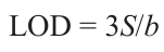
where S is the standard deviation of the blank signal, and b is the slope of the calibration plot. The calculated LOD was 0.2 μM, while the maximum sensitivity was 1941 μA mM–1 cm–2 for hydrogen peroxide. Meanwhile, the calculated limit of detection of D-glucose was 2.2 μM, and the maximum sensitivity was 1711 μA mM–1 cm–2. The low limit of detection for the considered analytes demonstrated by cobalt-doped copper structures can be attributed to the large specific surface area of the material. In addition, the high sensitivity of the copper – cobalt electrode may be due to the electrocatalytic interaction between copper and cobalt. As indicated above, this interaction is due to the peritectic nature of interaction reflected in the Cu – Co binary diagram. A similar result was obtained for the Cu–Ag eutectic system. A comparison with Cu – Ni and Cu – Fe bimetallic deposits showed that the eutectic nature of the phase diagram is a crucial factor for the formation of improved sensing properties of a bimetallic system formed by LCLD.[43][81] Comparison of the LCLD sensor parameters with the characteristics of other sensor materials is presented in Table 2 and Table 3.[102][182-198]
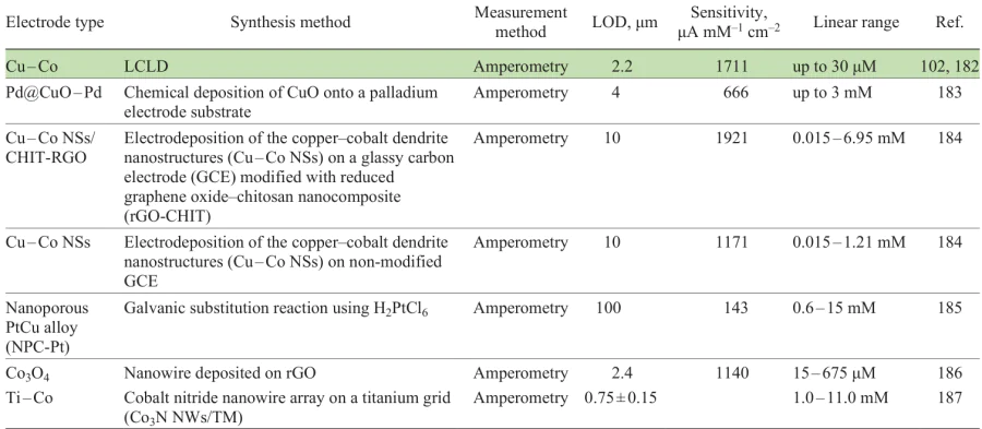
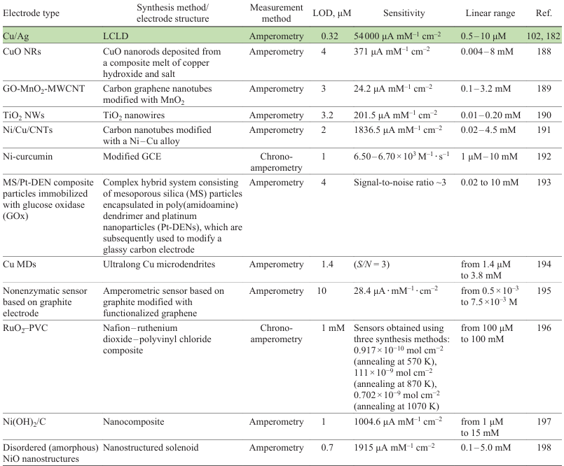
Smikhovskaia et al.[182] reported the preparation of a heterogeneous highly sensitive layer in the Cu – Ag system by two methods: co-deposition of Cu and Ag (Cu + Ag) and successive deposition: predeposition of pure Cu and deposition of the Ag nanoprecipitate onto the copper layer (Cu/Ag). The latter method proved to be much more effective for the production of a highly sensitive sensing layer. In Table 3, this sensor is compared with analogous sensors obtained by other traditional methods.
LCLD sensors based on bimetallic deposits and the prospects for their application were reported also in another study by Smikhovskaia et al.[199] The authors markedly extended the range of copper-based metallic and bimetallic nanostructures with sensing properties for biological analytes and demonstrated the superiority of copper–cobalt systems over other binary systems. Lebedev et al.[200] reported modification of porous glass membranes with gold nanoparticles using LCLD. This method provides the possibility, in the future, to design membranes with unique properties for the selective separation of complex biological mixtures, thus facilitating their analysis by traditional analytical chemistry techniques.
7. Catalytic properties of deposits formed by PLD and LCLD methods
A great portion of PLD nanostructures are developed as catalysts for water splitting to produce oxygen and hydrogen. A brief review of these studies shows that the most pronounced effect is generally achieved using heterogeneous catalysts, i.e., surfaces in which fluctuations in the chemical composition occur as clear-cut boundaries that accumulate a partial positive or negative charge accessible for transfer across the aqueous medium. Thus, the cathode and anode in the electrochemical water splitting reaction appear owing to the confining electrical double layer at the interfacial contact rather than owing to an external potential difference; this makes these catalysts highly effective.
Du et al.[201] described the use of perovskite oxide nanofilms as a considerably improved electrocatalyst for the production of oxygen in alkaline solution. The PLD method was used to manufacture the heterophase SrCo0.85Fe0.1P0.05O3 material on nickel foam (SCFP-NF). The authors obtained a catalyst with a large number of active sites and high electrical conductivity. The PLD method generates active sites from the oxygen vacancies on the perovskite nanofilm surface, which gives rise to a high concentration of atomic oxygen O22−/O−. The resulting SCFP-NF catalyst with a low mass loading (≈ 30 μg cm–2) exhibits high activity in the oxygen evolution reaction (OER) with a low overpotential of 290 mV and has excellent stability for up to 200 h at 10 mA cm–2 in an alkaline medium. The catalytic activity of this perovskite nanofilm surpasses that of most known metal oxide catalysts and the benchmark RuO2.
Fominski et al.[202] studied characteristics of hydrogen evolution reaction (HER) catalyzed by the highly extensive surface of thin MoSx layers formed by grazing incidence pulsed laser deposition (GI-PLD). During GI-PLD, a few large particles were accumulated on the substrate that was arranged along the direction of the laser plume (Fig. 16).
![[{"id":"iMirmzxCOc","type":"paragraph","data":{"text":"Schematic diagram of the formation of nanostructured films by grazing incidence pulsed laser deposition (GI-PLD) method:<sup>202</sup> (<i>1</i>) laser radiation source, (<i>2</i>) high-energy-density beam, (<i>3</i>) focusing system, (<i>4</i>) target (MoS<sub>x</sub>), (<i>5</i>) ablation plume, (<i>6</i>) flux of target nanofragments, (<i>7</i>) substrate, (<i>8</i>) nanolayer of material of the target, (<i>9</i>) direction of laser plume movement, (<i>10</i>) inert gas (Ar) chamber."}}]](/storage/images/resized/4Q3v35LTPKauPfQkgSfD70mnELh4DKloWpAs1Vk6_xl.webp)
The local structure and composition of thin MoSx layers formed by the deposition of the gas component of the laser plume were varied by changing the pressure of the buffer gas (in this case, Ar). An increase in the gas pressure led to the formation of quasi-amorphous MoSx (x ≥2) films, which possessed highly active catalytic sites at the boundaries of the layered MoS2 nanophase. This was accompanied by a decrease in the MoSx deposition rate due to scattering of the ablation plasma flux by Ar molecules during flux transport from the target to the substrate. This effect prevented the uniform deposition of the catalytic MoSx film onto the surface of most nanoparticles.
This was caused by the fact that the deposition rate of the nanoparticles did not depend on the Ar pressure, whereas scattering of MoSx consisting of a diffuse flux of Mo and S atoms did depend on the pressure of argon. Exactly these atoms served as the sources of MoSx film growth during GI-PLD. The thickness and composition distribution of the MoSx film on the substrate depended not only on the buffer gas pressure, but also on the distance to the target. At a distance of 1.0 – 2.5 cm from the target, the deposition rate was quite sufficient to form sulfur-enriched quasi-amorphous MoSx catalytic films (2.5 < x < 6) consisting of close-packed nanoparticles of 30 – 50 nm size.
At the first glance, this is the description of deposition of a single-phase coating with high catalytic properties. However, certain remarks made by the authors give a clue that, in this case, they were dealing with amorphized heterophase structures because of disruption of the stoichiometry in the plasma flux, giving rise to interfaces between MoSx layers of various compositions. This is evidenced by the fact that GI-PLD films had a higher density of catalytically active sites with a distinct local atomic configuration, including edge sites of the layered MoS2 nanophase and various S ligands in the amorphous phase containing Mo – S3 clusters. For a moderate loading of ∼ 300 μg cm–2 on glassy carbon substrates and overpotential of –140 mV, these films activated the H2 formation with geometric current densities of up to –10 mA cm–2.
The electrochemical water splitting is a promising process for the efficient production of green hydrogen. However, the overall efficiency of typical devices is often reduced due to the slow kinetics of the two half-reactions, especially the oxygen evolution reaction at the anode. Therefore, considerable research efforts are concentrated on the development of highly efficient electrocatalysts for oxygen extraction. The discrepancy between the bulk and surface properties of the catalysts, including their composition and electronic and geometric structures, complicates accurate identification of the relationship between the structure and performance.
Catalysts based on SrIrO3 thin films have been developed.[203] Iridium-based perovskite type oxides are highly active acidic electrocatalysts for OER responsible for the selective leaching of cations from the anode during OER. The porous Ag-PLD catalyst also demonstrated high activity in OER with a good onset potential (1.007 V) and half-wave potential (0.863 V), outperforming the reference commercial Pt/C catalysts and most known Ag-based catalysts.
An alternative to phase separation in PLD films is to enhance the defectiveness of the surface by other methods that increase the number of molecular-sized point defects per cm2 of the surface. Swaminathan et al.[204] obtained highly defective films of non-stoichiometric titanium dioxides (TiO2.40, TiO1.81, TiO1.74, TiO1.72, and TiO1.54) using a scalable precision pulsed laser deposition technique. The catalytic activities of the products were compared with that of stoichiometric commercial TiO2 (Degussa P25). The simple lowering the O/Ti ratio transforms titanium dioxide from a photoelectrocatalyst into an electrocatalyst for intense decomposition of water. When the composition is TiO1.81, titanium dioxide acts as a photoanode for reactions involving oxygen vacancies and generates a photocurrent of 0.62 mA cm–2. As the number of oxygen vacancies in titanium dioxide increases, there is a relative increase in the intensity of electrocatalytic hydrogen evolution, providing a current density of 10 mA cm–2 at an overpotential of only 610 mV. The concentration of defects in titanium dioxide largely determines the trade-off between electrocatalytic and photoelectrocatalytic behaviour during water splitting. The higher photoelectrocatalytic activity of TiO1.81 in water splitting is due to its high microstrain (1.9%) related to lattice distortions caused by defects. Meanwhile, high density of oxygen vacancies in TiO1.54 induces a pronounced lattice distortion in the TiO6 octahedra, with a small microstrain of 0.4%, which ensures a high density of negatively charged sites (10.2 × 1018 cm−3) and promotes efficient electrocatalytic water splitting. Generally, this work highlights previously unexplored and untapped aspects of PLD defect engineering.
Heterophase electrocatalysts based on mixed transition metal oxides are used for the electrochemical oxidation of water. The practical application of mixed oxides is justified by their low cost. These oxides include Co – Fe – B – O coatings synthesized by PLD for the electrochemical oxidation of water.[205] The catalytically active surface of such oxides exhibits an urchin-like (according to the authors) nanomorphology. Spiky three-dimensional particles are embedded between crystallized single-phase CoFe2O4 nanowires. This generates the effect of a large specific surface area. Nevertheless, the large surface area provides a lower catalytic activity than that of boron-containing quasi-heterophase core – shell particles of the same system. These are particles composed of a boron-containing core coated with a metal oxide film. A heterophase contact arises between the core and the shell. The films composed of these particles exhibit higher electrochemical activity toward water oxidation in an alkaline medium than urchin-like structures, with the overpotential being 315 mV at 10 mA cm–2. This is in line with a similar effect observed with catalysts synthesized by the LCLD method[7][147] and with the results obtained by Siebenhofer et al.,[206] who revealed the causes for the formation of charged defects in the system. In this case, Co is the active element, boron prevents the complete Co oxidation to give Cо2+ active species (CoOOH), while Fe promotes the reduction of Co3+ to Co2+. Testing of both structural types of the synthesized catalytically active Co – Fe – B – O films demonstrated good stability, which is one of the key characteristics required for practical applications.
Another promising application of PLD technique is selective organic catalysis.[207] [208] An ultrathin Ag film with a thickness of up to 300 nm was produced on a quartz substrate by pulsed laser deposition. A target made of pure silver was used. The synthesis was carried out at room temperature using a film thickness monitor. The resulting material can be used as a selective and portable nanocatalyst for the decomposition of hazardous organic compounds. The film obtained by PLD has polycrystalline cubic structure. The sample was tested as a catalytic nanocoating for the reduction of 4-nitrophenol to 4-aminophenol and demonstrated excellent catalytic performance, with 80% of the compound being reduced in only 1 h. The process using NaBH4, which had been employed previously required 5 to 6 times more time.
The PLD method was used[209] to fabricate a ZnO thin film for photocatalytic applications. The film had a uniform morphology with a grain size of less than 100 nm and a wurtzite hexagonal crystal structure. The band gap energy of this semiconductor material was 3.25 eV. The photocatalytic activity of the film was tested in the decomposition of Rhodamine B (RdB) in solutions of varying concentrations over a period of 6 h under simultaneous exposure to sunlight. The concentration of RdB decreased by 9% compared to the initial concentration, which, in the authors’ opinion, indicates that the film is a good photocatalyst for organic reactions. In our view, on the contrary, the outcome does not look very promising. For example, thin heterophase highly defective Cu2ZnSnS4 (CZTS) films with thicknesses of 61, 112, 242, and 313 nm obtained[210] by PLD on sodium calcium glass substrates showed a much better photocatalytic activity. The effect of film thickness on the activity is due to the porous structure of the surface.[210] An increase in the film thickness increases the specific surface area, but after a certain limit, diffusion limitations come into action, preventing the analyte from penetrating into the deeper layers of the film. Therefore, the 242 nm-thick CZTS photocatalyst showed the highest performance: it provided removal of 96.1% of Methylene Blue (MB) from a solution over a period of 4 h. The low efficiency of the material reported by Yudasari et al.[209] is caused by the single-phase, homogeneous structure of the catalytic photomaterial and a small number of surface defects.
Active experiments with deposits formed by LCLD aimed at the development of selective catalysts for organic synthesis are in progress.[21][80][149] Considering the in situ laser deposition of copper in the reaction mixture for the Sonogashira reaction, Fromme et al.[149] showed that two types of action of active LCLD catalyst are possible under laser irradiation: steady-state and dynamic ones (Fig. 17).
![[{"id":"hfM-LuN9HZ","type":"paragraph","data":{"text":"The successive stages of laser catalysis. (<b>1, 2</b>) dynamic; (<b>3</b>) steady-state ones; (<b>4</b>) substrate, laser beam, and the deposited track of metal nanostructures with various thermal zones (<b>1</b> is the high-temperature zone, <b>2</b> is the medium-temperature zone, <b>3</b> is the low-temperature zone)."}}]](/storage/images/resized/qEsLmjiKYzsllmbd4UHtbpJNRu2Cn9zRyqP1JWq5_xl.webp)
In the steady-state regime, catalysis in zone 3 takes place on the metal that has already been deposited by LCLD. In the dynamic regime, catalysis in zones 1 and 2 takes place during the formation and active growth phase of the nuclei under direct laser irradiation and during the subsequent growth of nano- and microcrystals in the high- and medium-temperature zones. The choice of the selectively catalyzed reaction among the possible reactions for a specified composition of the reaction mixture was based on the size of the metal nanoparticles formed by the instant of catalysis. This size, in turn, is determined by the concentration of metal salts in the reaction mixture and the presence of components that restrict or promote the growth of nano- and microcrystals in the catalyst. In the initial stage of nucleation and formation of nanoparticles under conditions of intense photoemission and high temperature, water splitting reaction and dehydrogenation of organic components of the aqueous solution take place, which is the dynamic catalysis stage. The size of the catalytic nanoparticles for these reactions ranges from 10 to 50 nm. As the particle size further increases and the catalysis conditions become milder, in particular the temperature decreases and the photoemission processes are absent, decomposition reactions of organic components present in the aqueous reaction mixtures start to proceed. These reactions give unsaturated hydrocarbons and hydrogen, e.g., light unsaturated hydrocarbons
Then reactions on metal nanoparticles take place (n = 7 – 20)
The size of catalytically active nanoparticles for these reactions ranges from 50 to 100 nm. Low-energy reactions (characterized by low reaction enthalpies) start at low temperatures about 20°C in the steady-state catalysis zone. They include, for example, the homocoupling reaction (particle size of 100 – 200 nm), the Sonogashira cross-coupling reaction (200 – 400 nm), and other.
The following trends were revealed for the results of laser treatment of the reaction mixtures containing components of organic synthesis:
— the organic components present in the aqueous solution during the continuous generation of the laser catalyst can simultaneously act as reducing agents for the laser reaction and as precursors for catalytic decomposition reactions to give hydrogen and unsaturated hydrocarbons;
— catalysis of organic reactions (both destructive and constructive ones) by laser-induced catalysts takes place on the growing nanoparticles of the deposited metal deposit both when the reaction mixture is irradiated with a laser and after the laser beam has been switched-off. The laser-deposited metal structures exhibit catalytic activity during the equilibrium phase of crystal growth until they reach thermodynamic equilibrium with the reaction mixture components and the catalytic surface is poisoned by reaction products.[21][211] The crystal growth is accompanied by a decrease in the specific surface area and in the number of surface defects carrying a partial charge.
A series of experiments on the catalytic conversion of ethanol in water in the presence of an aqueous solution of copper chloride [212-214] led to synchronous change in the concentrations of complete and partial dehydrogenation products (hydrogen, ethanal, ethylene, and methane) upon switching on and off laser radiation. A study of the time variations of component concentrations in the gas phase directly during the laser deposition for all of the solutions also revealed a direct relationship between their appearance in the gas phase above the solution and the presence of laser radiation (Fig. 18).[214]
![[{"id":"mFA0YAjX8b","type":"paragraph","data":{"text":" (<i>a</i>) Time variation of the intensity of the characteristic lines of some components of the gas phase above the aqueous solution in which the LCLD reaction takes place. (<i>b</i>) Scaled-up plot for ethylene. Deposition was performed from the following solution: CuCl<sub>2</sub> (0.020 М), EDTA (0.088 М), NaOH (0.1 М).<sup>214</sup>"}}]](/storage/images/resized/Tbsc0QsdR4bPSZuXt2vawoohNkTBeSkKPG5JrDJG_xl.webp)
8. Conclusion
The role of interfacial interactions in the design of catalytically and sensor-active materials using laser deposition methods is very well illustrated by Seo et al.[82] In 2020, the authors of that study, who addressed the deposition of conductive copper tracks on silicate glass, attempted to reproduce the techniques used by the pioneers of this method, A.G.Shafeev[61-63] and Kordás.[60]
Recall that the preactivation of single-phase dielectric surfaces, including glass, polyimide, etc., prior to laser deposition was performed to produce high-quality metal tracks. In the works of A.G.Shafeev and other researchers of that time, the main criteria of quality were the continuity and good adhesion of the tracks to the substrate, combined with high electrical conductivity comparable to that of monolithic metal. Several methods were used: mechanical action such as polishing, scratching (scribing) by a solid material, and chemical and laser etching. In the two first-mentioned cases, the improvement of the quality of tracks was mainly achieved by increasing the specific surface area of the dielectric substrate. Thus, the number of activated surface sites increased in proportion to the increase in the surface area, but their concentration remained unchanged. Laser preactivation considerably increased the concentration of activated sites in the zone of laser beam action. This activation also persisted after the laser radiation was switched off; in some cases, this made it possible to deposit metal tracks onto the laser trace in a second step simply by placing the activated substrate into a solution for laser deposition. However, even this expedient did not produce tracks with a stable quality that would ensure practical application. Glass is a well-known non-conductive material, which is used, in particular, in electronics. It is not surprising that the deposition of copper onto a single-phase SiO2 surface resulted in discontinuous tracks on the glass surface and that there were problems associated with track detachment from the substrate due to the relatively low adhesion of the deposited copper to the untreated glass surface. The picture of deposition closely resembled the illustration given in Fig. 5 of this work. Following the work of A.G.Shafeev, the authors attempted to perform laser preactivation of glass prior to the deposition of the conductive track in order to increase the specific number of activated sites. In A.G.Shafeev’s works, preliminary laser activation of SiO2 was performed by the PLAL technique. In the cited study, laser-induced backside wet etching (LIBWE) was used for activation (Fig. 19).
![[{"id":"fXUXdKelEF","type":"paragraph","data":{"text":"Schematic diagram of the laser-induced backside wet etching (LIBWE). (<i>1</i>) laser radiation source, (<i>2</i>) laser beam, (<i>3</i>) focusing system, (<i>4</i>) transparent quartz glass substrate, (<i>5</i>) aqueous solution or pure water."}}]](/storage/images/resized/SS4o7ZsKQtjgYgXm0AESCnRqsZo69t1WBiDZZ9fp_xl.webp)
This process served for the preliminary generation of microchannels on the glass surface, which are subsequently filled with copped by means of LCLD. As a result of enhanced adhesion between the glass and the deposited copper, a ‘stronger copper wire’ was produced.[82] Apart from the use of the LIBWE method, adhesion was enhanced by a polished rough surface and the predeposited metal layer.
Considering the data analyzed in this review, the proposed method appears to be too complicated, time-consuming, and insufficiently effective. Meanwhile, the conventional silicate glass can be simply replaced by any silicate-based microcomposite such as ST-50.1 crystalline glass ceramics to obtain a versatile substrate that would fully retain the dielectric properties of SiO2 , but would still allow for the formation of metal tracks and films in one step using laser methods without the need for preactivation. This is evidenced by the large number of studies cited in this review.
The use of modern laser technologies to fabricate microelectronic components, sensors, and catalysts has become a global trend. The PLD and LCLD-PLAL methods are most practically feasible among numerous alternatives, as they allow for the automation of all operations, require minimum labour, and are highly environmentally friendly. They can be implemented using simple and inexpensive equipment that is mass-produced in many countries around the world.
To summarize the above information, we can identify a key chemical factor determining the production of new nanomaterials with a wide range of catalytic and sensing properties using laser deposition techniques in a vacuum, an inert gas atmosphere, or a liquid. The laser synthesis of nanolayers and nanoparticles possessing a set of desired properties is based on the principle of placing heterophase materials at the focus of a high-fluence laser radiation. The new nanomaterials produced in this way also exhibit high catalytic and sensing activity if a heterophase nanocomposite material has been formed.
The control over laser deposition processes develops along two lines: generation of highly defective extensive surfaces and films for the synthesis of nanomaterials and optimization of the composition of solutions for laser deposition. Both processes prove to be effective if the principle of material heterogeneity is applied. In other words, the deposition of heterophase catalytic and sensing materials proceeds most effectively on heterophase surfaces. This is due to the formation of microzones in which a potential drop arises causing a cathode–anode or donor–acceptor reaction. The surface sites act as catalysts for chemical reactions by lowering the activation energy of processes that are difficult to carry out under usual conditions. In the case of PLD and LCLD methods, catalysis occurs on active clusters formed via laser deposition processes and representing acceptor or donor type defects, that is, in terms of physics, defects that can be negatively or positively charged, respectively. The oxides of metals that can form cations in different oxidation states and exist as both cationic (M+) and anionic (MxOy)n– species are widely used as active oxidation catalysts.
The existing processes for the production of catalysts for selective organic synthesis typically use expensive metals such as gold, platinum, palladium, etc.[215][216] This results in high cost of catalysts and synthesis processes using these catalysts. The main challenges associated with the use of less expensive metals such as copper, cobalt, silver, etc. are fast poisoning of the catalyst surface by reaction products and the loss of activity.[217][218] The regeneration of spent catalysts and the synthesis of new ones is a labour-intensive and costly process. Catalysts based on non-precious and non-rare-earth metals prepared using LCLD are characterized by long service life in the reaction mixture, which is limited only by the laser lifespan. The LCLD reaction gives rise to metallic structures that may possess catalytic properties similar to those of copper–rhenium analogues.[219]
The possibility of large-scale production of electrocatalysts using the pulse deposition method is also an important topic for discussion. Global supply of PLD systems remains limited, mainly due to the high cost of excimer lasers, but their wider distribution will make PLD more accessible to many researchers and manufacturers.
This study was performed with the support of the Ministry of Education and Science of the Russian Federation (Project FSRM-2026-0027).
9. List of abbreviations
CNMs — (ultrapure) carbon nanomaterials,
CVD — chemical vapour deposition (a method for production of target deposits from the gas phase containing atoms and molecules of precursors),
CV — cyclic voltammetry,
GI-PLD — grazing incidence pulsed laser deposition,
HER — hydrogen evolution reaction,
LCLD — laser-induced chemical liquid-phase deposition,
LIBWE — laser-induced backside wet etching,
LIFT — laser-induced forward transfer,
LOD — limit of detection (the concentration limit of analyte detection with a sensing surface of a sensor),
Nd:YAG — neodymium yttrium aluminium garnet (laser type often used for pulsed laser deposition processes),
ORR — oxygen reduction reaction,
PLAL — pulsed laser ablation in liquid,
PLD — pulsed laser deposition,
RoHS — (European Union) Restriction of Hazardous Substances,
SCE — saturated calomel electrode,
ST-50-1 sitall (crystalline glass ceramics) — microcomposite of rutile (α-TiO2) and cordierite (2MgO · 2 Al2O3 · 5 SiO2),
XRD — X-ray diffraction,
b — width of the track laser-deposited on a substrate or film fragment width,
D (nm, μm) — thickness of films and deposits formed on the substrates upon laser deposition,
J (W cm–2) — laser fluence,
I — reduced intensity of a laser beam,
K — slope of the dependence of the track width b on the laser radiation power W,
KB — Boltzmann’s constant,
k — number of active sites per unit area of the substrate surface,
L (μm, mm) — length of all interfaces over an area of 1 cm2,
P (Pa) — gas pressure in the pulsed laser deposition chamber,
R — rate of material deposition on a substrate during laser deposition processes,
𝑟 — distance between the focal point of the laser beam and the point with the coordinates X, Y,
S — standard deviation of the sensor signal,
Uv — volume fraction of the phase with the degree of dispersion V,
V — degree of dispersion of a phase,
v — laser beam velocity relative to the substrate,
W (W) — laser radiation power,
xp and yp — coordinates of the centre of the plume relative to the substrate centre in the PLD technique,
z — distance between the target and the substrate in the PLD technique,
δ — optical penetration depth ((attenuation length) of the laser beam in the deposit or substrate material,
λ — laser radiation wavelength,
rk — probability of the elemental step of formation of a k-atomic cluster per unit surface area and per unit time,
σ (S, Ω) — electrical resistance of a sensor before and upon exposure to a gaseous atmosphere,
τ (ns) — laser pulse duration (length).
References